Method for measuring circuit board line width based on largest communication domain

A technology with the largest connected domain and measurement method, applied in measurement devices, image data processing, instruments, etc., can solve the problems that automatic measurement cannot be achieved, and it is difficult to accurately and automatically find the edge of a straight line, so as to achieve automatic measurement and improve measurement accuracy. and stability effects

Inactive Publication Date: 2008-11-12
NANCHANG HANGKONG UNIVERSITY
View PDF0 Cites 34 Cited by
  • Summary
  • Abstract
  • Description
  • Claims
  • Application Information

AI Technical Summary

Problems solved by technology

The existing image-based circuit board line width measurement method can realize automatic measurement for circuit boards with large contrast between straight lines and substrates, such as inner copper plates, and has high measurement accuracy, but for external circuits with small contrast between straight lines and substrates Copper plate, it is difficult to accurately and automatically find the edge of the straight line, and automatic measurement cannot be realized, usually measured by manual method

Method used


Image

  • Method for measuring circuit board line width based on largest communication domain
  • Method for measuring circuit board line width based on largest communication domain
  • Method for measuring circuit board line width based on largest communication domain

Examples


Embodiment Construction

[0031] The input image data used for measurement in the present invention comes from two ways: one is a single-frame image obtained by using a microscopic zoom camera through an image acquisition card, and the other is an image file in two formats of .BMP and .JPEG. Image formats can be 8-bit grayscale, 24-bit and 32-bit true color images. Video input can be PAL or NTSC standard video signal.

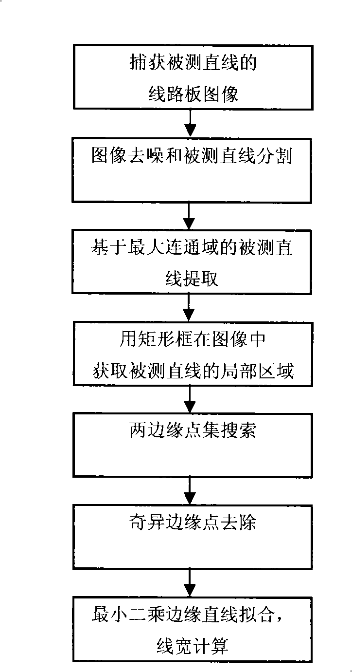
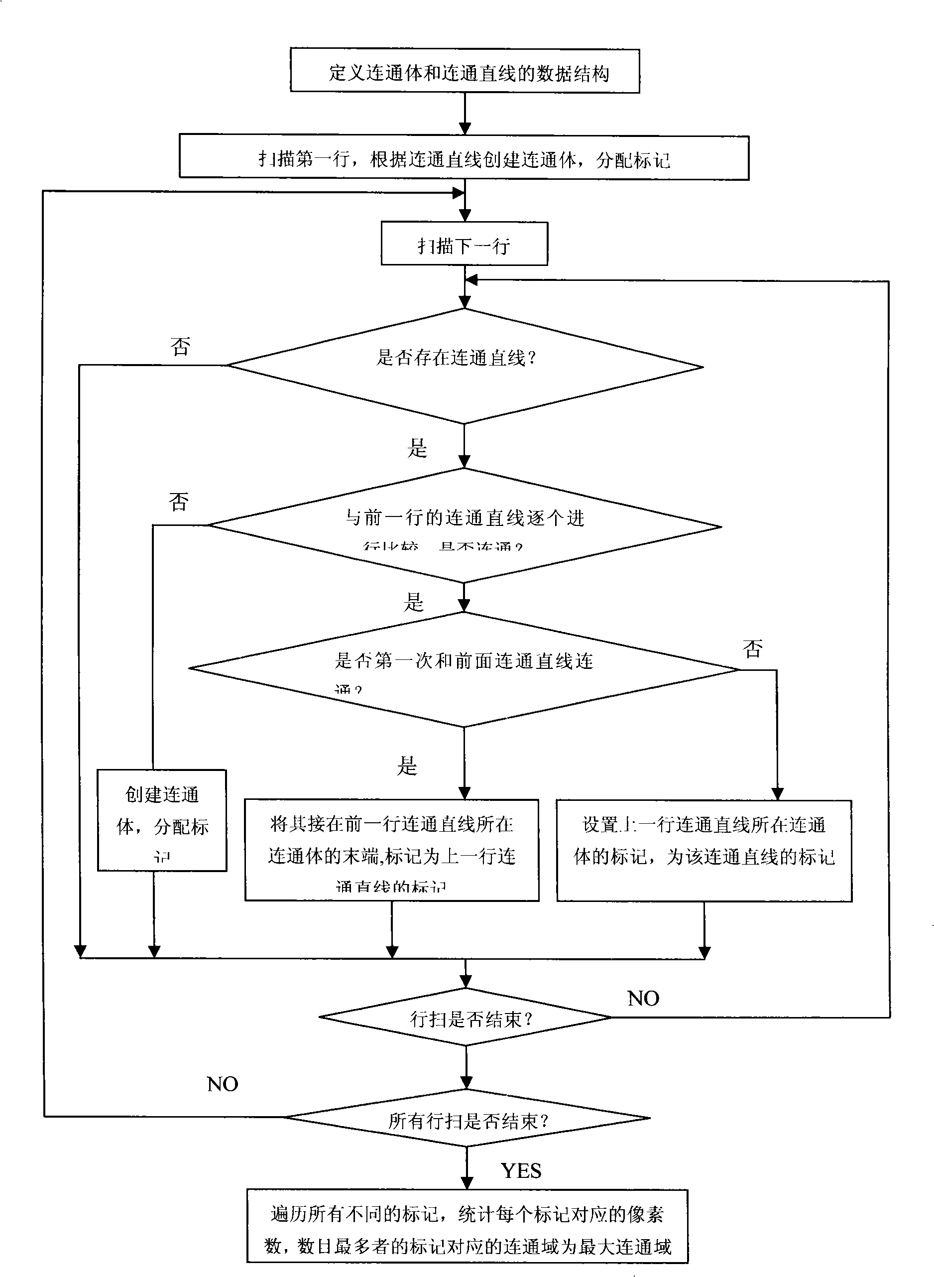
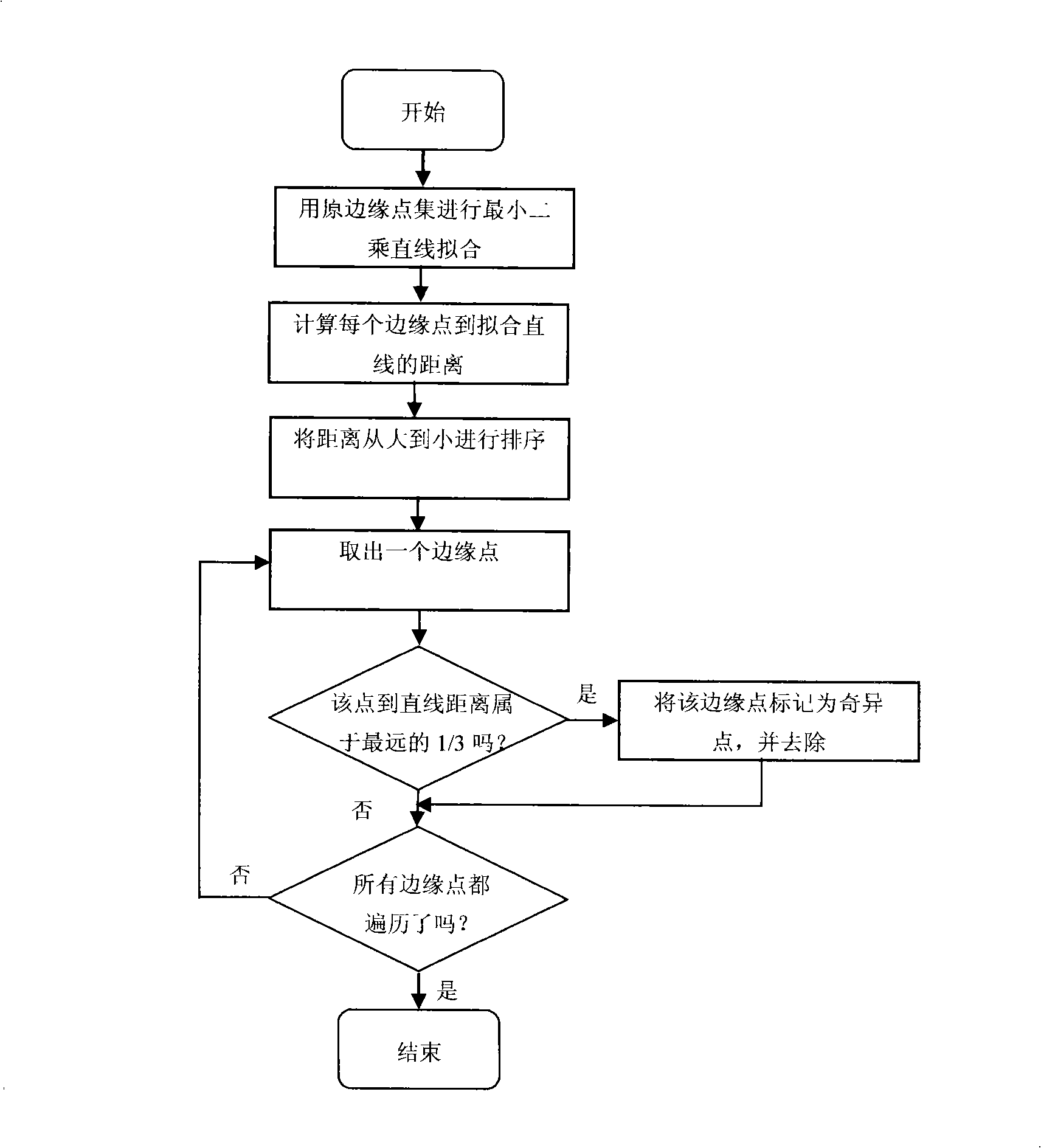
[0032] For an image, the method mainly includes capturing the circuit board image of the measured line, denoising the image and segmenting the measured line, extracting the measured line by using the maximum connected domain method, and determining the two edge point sets of the measured line by using the scanning method , removing singular edge points, using the least squares method to fit two edge straight lines and line width calculation steps, the work flow of the present invention is as follows figure 1 As shown, the specific implementation is as follows:

[0033] 1. Capture the ...


PUM


Abstract

The invention relates to a method for measuring line width of a circuit board based on maximum connected domain, which comprises the steps of: 1) capturing the image of a target circuit board; 2) denoising the image and segmenting a target straight line; 3) extracting the straight line by using the maximum connected domain method within a rectangular frame; 4) determining the point sets of both edges of the target straight line by scanning; 5) removing singular edge points; and 6) fitting the two edges of the straight line and performing line width calculation by using the least square method. By introducing maximum connected domain search for acquiring target straight lines, the method of the invention is applicable to line width measurement for not only interior copper plates but also exterior copper plates with small contrast between circuit and substrate. And by employing image denoising and singular point removal, the method achieves accurate acquisition of edges of target straight lines, and as a result, improved precision and stability of line width measurement.

Description

technical field [0001] The invention relates to a circuit board detection method, in particular to a circuit board line width measurement method based on the maximum connected domain. Background technique [0002] The miniaturization of integrated circuit (IC) chips has put forward higher requirements for the production of printed circuit boards (PCBs) with denser line widths and multi-layered layers. If the line width of the dense parallel straight lines on the PCB is too thick, it will easily cause a short circuit of the parallel lines; if the etching is too thin, it will easily cause abnormal signal transmission; ), it is easy to produce high-frequency reflection, form electromagnetic interference, and affect the stability of the electronic system. Accurate automatic measurement of straight line widths in printed circuit boards is key to high-quality circuit board fabrication. In the past, a magnification lens and a common quadratic element were usually used for measure...

Claims


Application Information

Patent Timeline
Patent Type & Authority Applications(China)
IPC IPC(8): G01B11/02G06T7/00
Inventor 熊邦书陈胜鹏王文进
Owner NANCHANG HANGKONG UNIVERSITY
Why Eureka
Try Eureka