Lead frame for leadless encapsulation, encapsulation construction and manufacture method thereof

A technology of packaging structure and manufacturing method, which is applied in semiconductor/solid-state device manufacturing, electrical components, electric solid-state devices, etc., and can solve problems such as area limitations

Active Publication Date: 2008-11-19
CHIPMOS TECH INC
View PDF0 Cites 1 Cited by
  • Summary
  • Abstract
  • Description
  • Claims
  • Application Information

AI Technical Summary

Problems solved by technology

However, the chip fixing pad 811 is located in the center of the pins 812, and must keep an appropriate distance from the surrounding pins 812, so the area is limited.

Method used


Image

  • Lead frame for leadless encapsulation, encapsulation construction and manufacture method thereof
  • Lead frame for leadless encapsulation, encapsulation construction and manufacture method thereof
  • Lead frame for leadless encapsulation, encapsulation construction and manufacture method thereof

Examples


Embodiment Construction

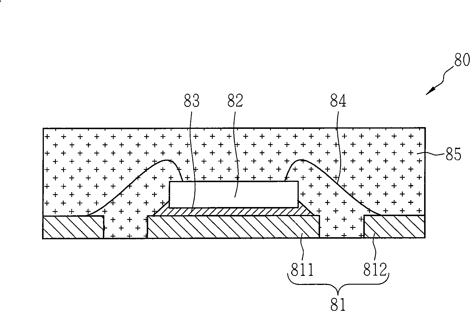
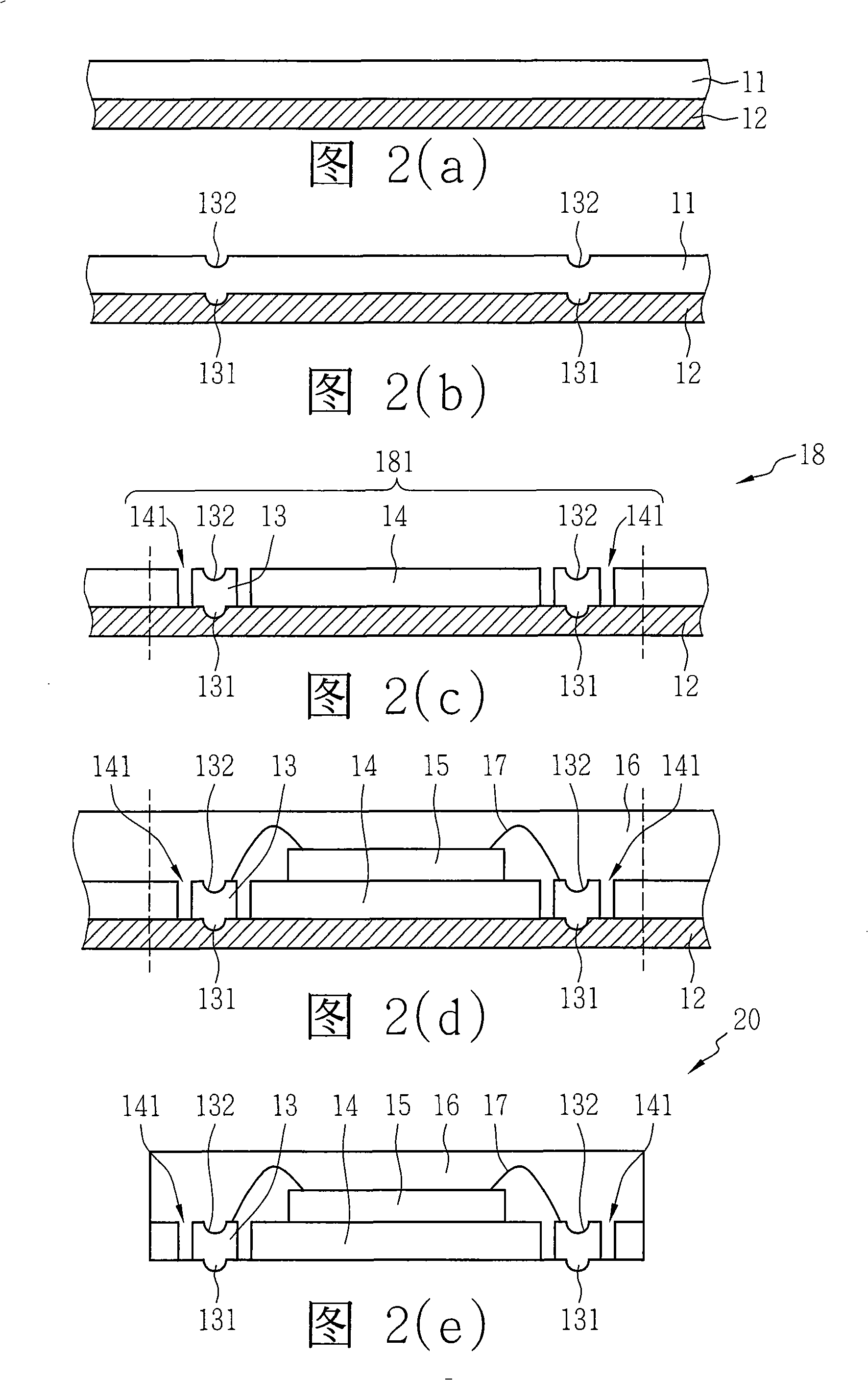
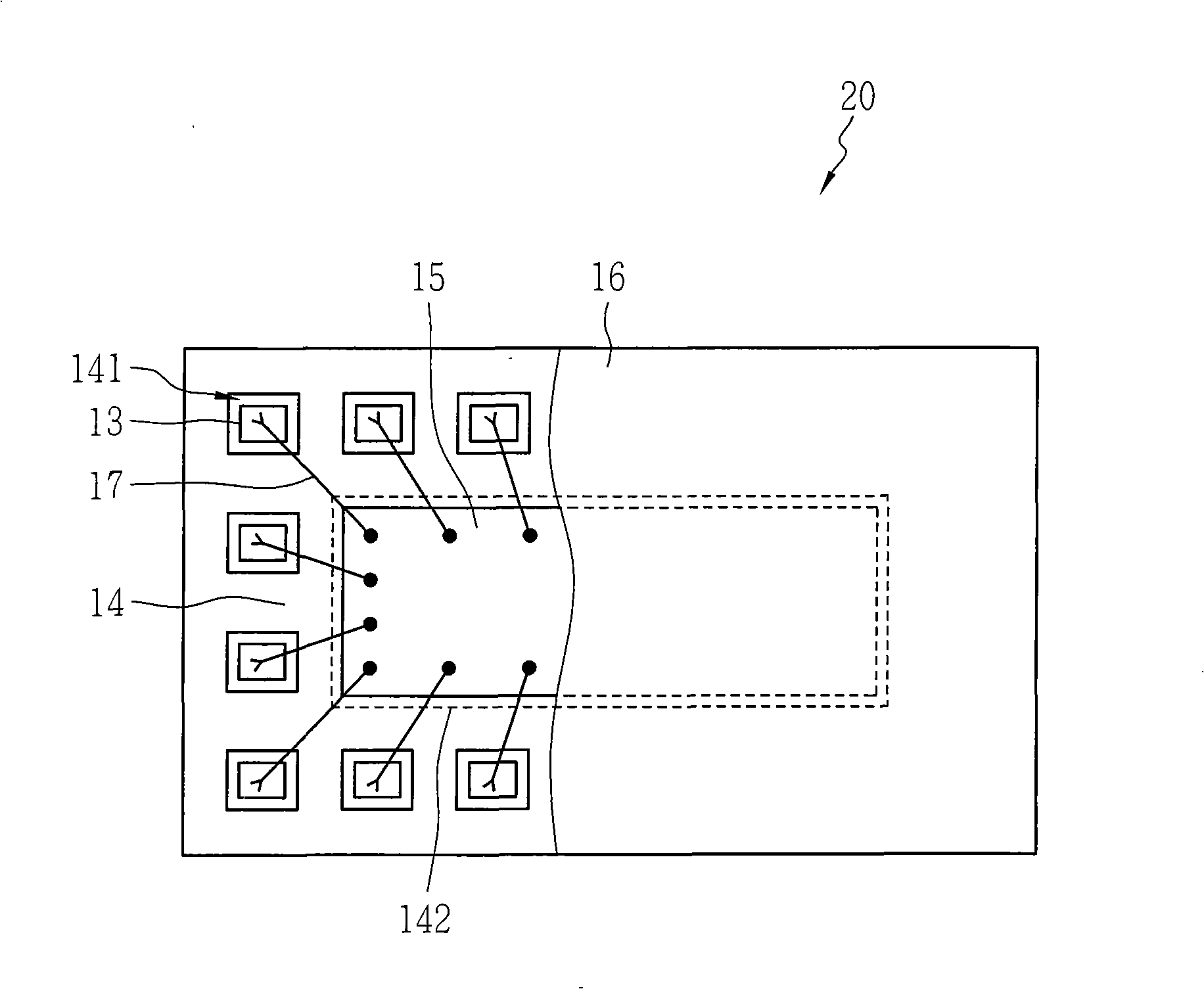
[0016] 2( a ) to 2 ( e ) are schematic diagrams of various manufacturing steps of the leadless package structure of the present invention. First, the metal plate 11 covered with the adhesive tape 12 is provided, and the metal plate 11 can be selected from the group consisting of copper, aluminum, copper-aluminum alloy, aluminum alloy and mixtures thereof. As shown in FIG. 2( b ), multiple depressions 132 are formed by stamping on the upper surface of the metal sheet 11 , and a plurality of protrusions 131 are produced on the lower surface of the metal sheet 11 bonded with the adhesive tape 12 . Then, the metal plate 11 is formed into a plurality of connected chip holders 14 and a plurality of separated pins 13 by photolithography, and the plurality of pins 13 are respectively arranged in a plurality of through holes 141 around each chip holder 14, As shown in Figure 2(c). Each die pad 14 and surrounding pins 13 are regarded as a package unit 181 on the lead frame 18 .

[001...


PUM


Abstract

The invention discloses a lead frame without a lead enclosure, which comprises a plurality of enclosing units and an adhesive tape. Each enclosing unit comprises a chip seat which is provided with a plurality of through holes, and a plurality of pins which are respectively arranged in the through holes. The adhesive tape is affixed to the surfaces of the enclosing units and fixes the chip seat and the pins.

Description

technical field [0001] The present invention relates to a lead frame for leadless packaging, its packaging structure and its manufacturing method, in particular to the structure of a quad flat non-leaded package (Quad Flat Non-leaded Package; QFN), the used lead frame and its manufacturing method . Background technique [0002] In order to comply with the trend of consumer electronics products emphasizing lightness, thinness and shortness, QFN packaging has surpassed traditional leaded packaging and is used to replace higher-cost wafer-level chip-scale packaging (wafer level CSP). Although chip-scale packaging (CSP) will package The shape is reduced to the size of the chip, but it is necessary to use an array of solder balls with a very close pitch as the component pins, which makes the product manufacturing more difficult. Compared with the QFN package, it is not only small in size, low in cost, and high in production yield, but also provides better coplanarity and heat di...

Claims


Application Information

Patent Timeline
Patent Type & Authority Applications(China)
IPC IPC(8): H01L23/495H01L23/488H01L21/50H01L21/60H01L21/56
CPCH01L2224/48247H01L2224/48091H01L2224/32245H01L2224/49171H01L2224/73265H01L24/97H01L2224/48465H01L2224/97H01L2924/181
Inventor 林峻莹沈更新潘玉堂周世文
Owner CHIPMOS TECH INC
Why Eureka
Try Eureka