Gan substrate, and epitaxial substrate and semiconductor light-emitting device employing the substrate

An epitaxial substrate and substrate technology, which is applied in the manufacturing of semiconductor devices, semiconductor lasers, semiconductor/solid-state devices, etc., can solve the problems of lower emission efficiency, lower device emission efficiency, etc., and achieve the effect of improving emission efficiency.

Inactive Publication Date: 2008-11-19
SUMITOMO ELECTRIC IND LTD
View PDF0 Cites 23 Cited by
  • Summary
  • Abstract
  • Description
  • Claims
  • Application Information

AI Technical Summary

Problems solved by technology

Since the c-plane is a polar plane, it generates a piezoelectric field, which has been a cause of reduced emission efficiency of light emitting devices using GaN substrates
Especially in devices employing an indium-containing emissive layer, in order to achieve emission in the green region, the amplified lattice mismatch between this layer and GaN further reduces the device emission efficiency

Method used


Image

  • Gan substrate, and epitaxial substrate and semiconductor light-emitting device employing the substrate
  • Gan substrate, and epitaxial substrate and semiconductor light-emitting device employing the substrate
  • Gan substrate, and epitaxial substrate and semiconductor light-emitting device employing the substrate

Examples


Embodiment 1

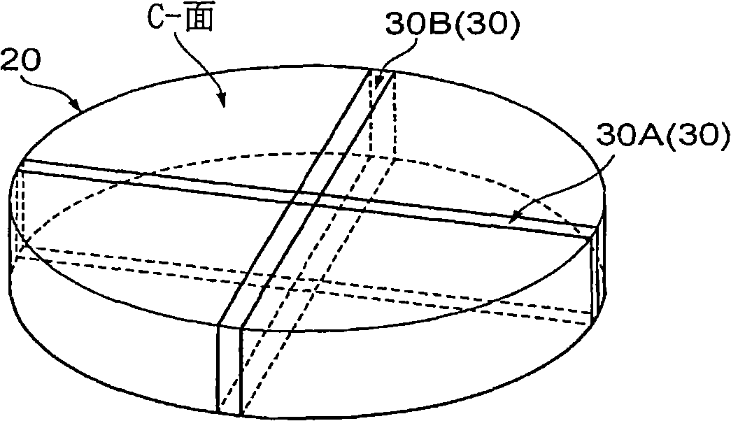
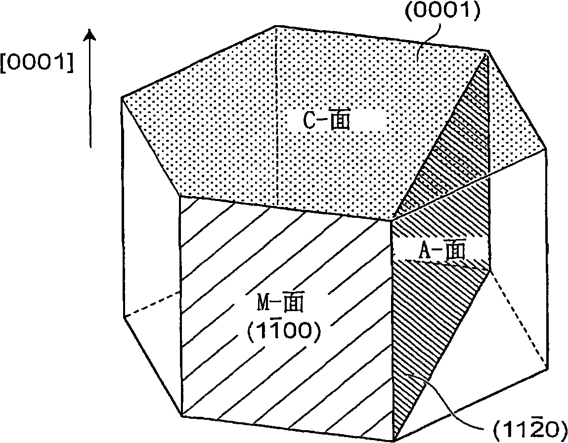
[0039] First, GaN substrate samples 1 to 14 were prepared according to the same process as the above-mentioned embodiment mode, which were the same or equivalent to the above-mentioned GaN substrate 30A-GaN substrate 5mm×20mm, the difference is that, as shown in the following Table I, Off-axis angle relative to the m-plane. In particular, among samples 1-14, the mis-orientation axis of samples 1-7 was the direction, and among samples 8-14, the mis-orientation axis was the direction. It should be noted that the crystal plane orientation (off-axis angle) of the GaN substrate is characterized by X-ray diffraction, and the measurement accuracy of the off-axis angle is ±0.01 degrees.

[0040] Table I

[0041] off-axis angle

0.00

0.03

0.1

0.3

0.5

1.0

2.0

direction

sample 1

sample 2

sample 3

Sample 4

Sample 5

Sample 6

Sample 7

direction

Sample 8

Sample 9

sample 10

Sample ...

Embodiment 2

[0056] In a manner similar to Example 1, GaN substrate samples 15 to 28 were prepared according to the same procedure as the previously explained embodiment mode, which were the same or equivalent to the above-mentioned GaN substrate 30B-GaN substrate 5mm×20mm, as follows Table IV, the difference is the off-axis angle relative to the a-plane. In particular, among samples 15-28, the mis-orientation axis of samples 15-21 was , and among samples 22-28, the mis-orientation axis was the direction. It should be noted that the crystal plane orientation (off-axis angle) of the GaN substrate is characterized by X-ray diffraction, and the off-axis angle measurement accuracy is ±0.01 degrees.

[0057] Table IV

[0058] off-axis angle

0.00

0.03

0.1

0.3

0.5

1.0

2.0

direction

Sample 15

Sample 16

Sample 17

sample 18

sample 19

Sample 20

sample 21

direction

Sample 22

Sample 23

Sample 24...


PUM


Abstract

The invention relates to a GaN substrate, an epitaxial substrate adopting the GaN substrate and semiconductor light-emitting devices. A growth plane (30a) of the GaN substrate (30) is oriented off-axis relative to an m-plane or an a-plane, namely in the GaN substrate (30), the growth plane (30a) is either the m-plane or the a-plane which has been misoriented. Because the m-plane and the a-plane are nonpolar planes, the GaN substrate (30) is utilized to manufacture the semiconductor light-emitting devices, so as to avoid the influence of piezoelectric fields so as to realize superior emission efficiency. The growth plane is imparted the off-axis angle according to the m-plane and the a-plane to realize high quality morphology in crystal grown on the substrate. Utilizing the GaN substrate to manufacture the semiconductor litght-emitting devices can further improve emission efficiency.

Description

technical field [0001] The invention relates to a GaN substrate, an epitaxial substrate using the GaN substrate and a semiconductor light emitting device. Background technique [0002] In the growth of crystalline GaN substrates, c-planes are usually used. Since the c-plane is a polar plane, it generates a piezoelectric field, which has been a cause of reduction in emission efficiency of a light emitting device using a GaN substrate. Particularly in devices employing an indium-containing emitting layer, in order to achieve emission in the green region, the amplified lattice mismatch between this layer and GaN therefore further reduces the device emission efficiency. (Refer to "Strain-Induced Polarization in WurtziteIII-Nitride Semipolar Layers," Journal of Applied Physics, vol.100, article023522, 2006 of A.E.Romanov et al.; "Demonstration of Nonpolarm-Plane InGaN / GaN Laser of Mathew C. Schmidt et al. Diodes, "Japanese Journal of Applied Physics, Vol.46, No.9, 2007, pp.L190...

Claims


Application Information

Patent Timeline
Patent Type & Authority Applications(China)
IPC IPC(8): H01L33/00H01L33/16H01L33/32
CPCH01L21/02502H01L33/32H01L21/02458H01L21/02389H01S5/32341H01L21/02433C30B29/406H01L33/16H01S5/3202C30B25/18H01L29/045H01L21/0254H01L21/20
Inventor 秋田胜史
Owner SUMITOMO ELECTRIC IND LTD
Why Eureka
Try Eureka