Semiconductor device, leadframe and structure for mounting semiconductor device

A semiconductor and lead frame technology, applied in the direction of semiconductor devices, semiconductor/solid-state device components, electric solid-state devices, etc., can solve the problems of no confrontation, etc., and achieve the effects of improving performance characteristics, reducing crosstalk interference, and narrowing the spacing

Inactive Publication Date: 2008-11-26
FUJITSU MICROELECTRONICS LTD
View PDF4 Cites 5 Cited by
  • Summary
  • Abstract
  • Description
  • Claims
  • Application Information

AI Technical Summary

Problems solved by technology

[0022] In this semiconductor device, as in the conventional device shown in FIG. 8, electrical interference occurs between the leads, but there is no countermeasure against the electrical interference.

Method used


Image

  • Semiconductor device, leadframe and structure for mounting semiconductor device
  • Semiconductor device, leadframe and structure for mounting semiconductor device
  • Semiconductor device, leadframe and structure for mounting semiconductor device

Examples


no. 1 example --

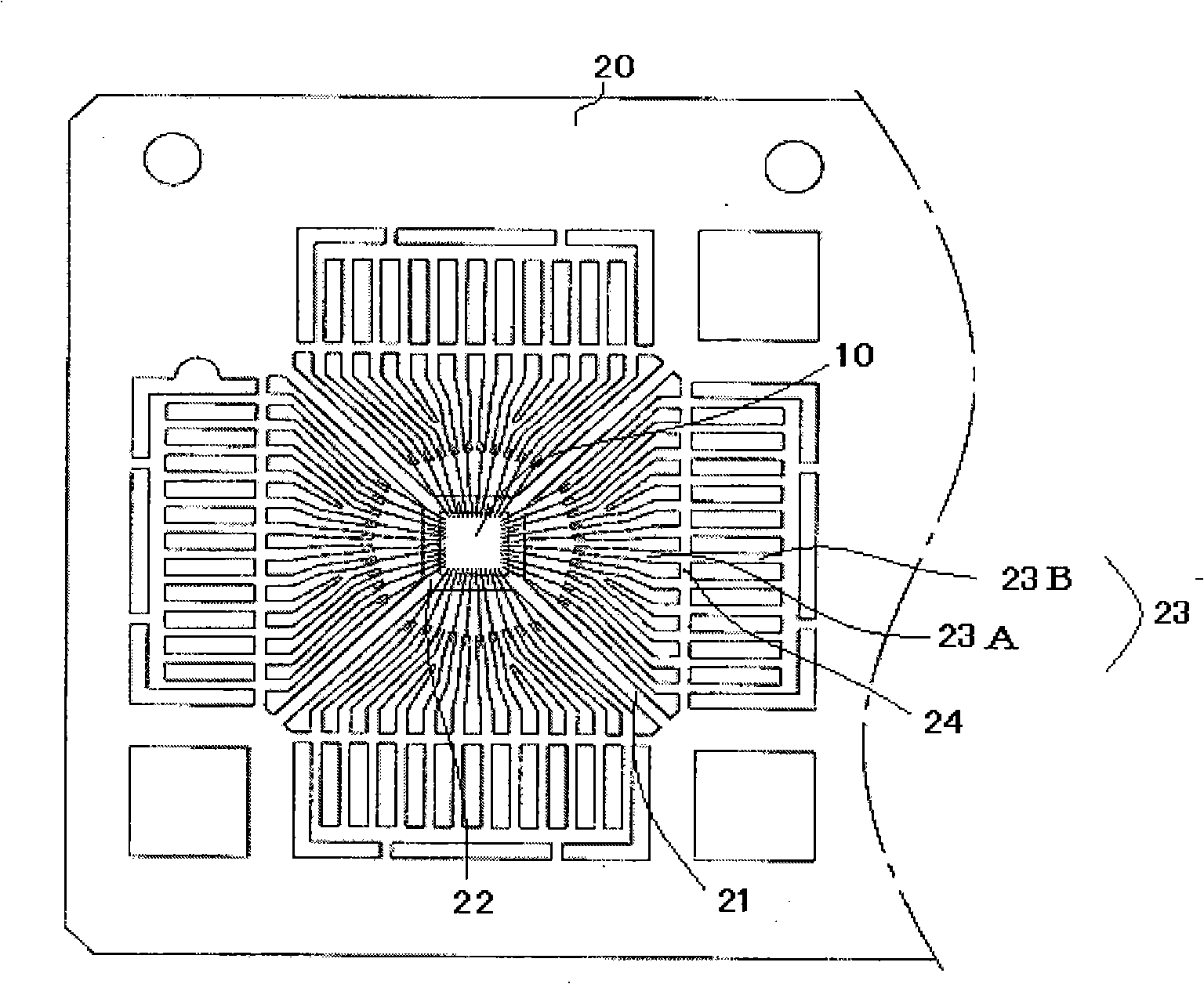
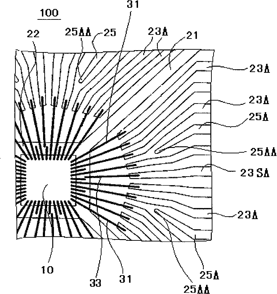
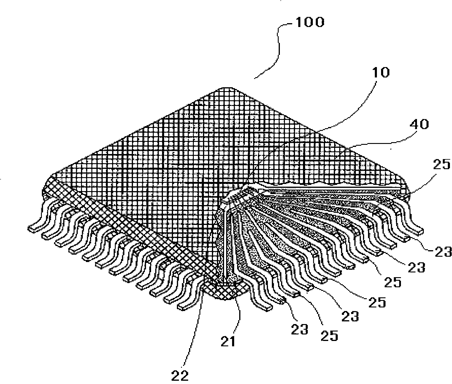
[0045] refer to Figure 1A , Figure 1B and figure 2 A first example of a semiconductor device according to the present invention, the semiconductor device 100, is described.

[0046] Figure 1A A lead frame of the semiconductor device 100 and an arrangement of semiconductor elements mounted on the lead frame are shown. Figure 1B show Figure 1A The main part of the magnification.

[0047] In this example, the semiconductor element 10 is mounted and attached to the rectangular die stage 22 of the lead frame 20 , and the four corners of the die stage 22 are supported by the die stage rods 21 . Electrode terminals of the semiconductor element 10 are connected to the leads 23 of the lead frame 20 through bonding wires 31 , and optionally connected to the die stage 22 .

[0048] A plurality of leads 23 (first leads) are arranged on substantially the same plane around the die stage 22 . Each lead 23 has a portion called an inner lead 23A and an outer lead 23B through a tie...

example 2

[0073] refer to Figure 3A and FIG. 3B depict a second example of a semiconductor device according to the present invention, a semiconductor device 200 .

[0074] Figure 3A A lead frame of the semiconductor device 200 is shown, and an arrangement of semiconductor elements mounted on the lead frame is shown. Figure 3B shows the Figure 3A The main part of the magnification.

[0075] Note that the same reference numerals are used for the Figure 1A , Figure 1B and figure 2 The components corresponding to the components of the semiconductor device 100 shown in FIG.

no. 1 example

[0076] Similar to the first example, the semiconductor element 10 is mounted and attached to the rectangular die stage 22 of the lead frame 20 , and the four corners of the die stage 22 are supported by the die stage rods 21 . Electrode terminals of the semiconductor element 10 are connected to the leads 23 of the lead frame 20 through bonding wires 31 , and optionally connected to the die stage 22 .

[0077] A plurality of leads 23 (first leads) are arranged on substantially the same plane around the die stage 22 . Each lead 23 has a portion called an inner lead 23A and an outer lead 23B through a tie bar (link) 24 . The inner lead 23A is closer to the die stage 22 (inner side) than the outer lead 23B located on the outer side.

[0078] Each inner lead 23A of the plurality of leads 23 is connected to an electrode terminal (such as a signal input / output terminal, a power supply terminal, or a ground terminal) of the semiconductor element 10 through a bonding wire 31 .

[007...


PUM


Abstract

A structure of a semiconductor device is provided, where intervals can be narrowed between leads arranged around a semiconductor element to increase the number of leads, and electrical interference is prevented or reduced between the leads to cause no crosstalk between the leads. The semiconductor device of the present invention includes a semiconductor element and a plurality of leads arranged around the semiconductor element. The plurality of leads includes a plurality of first leads and a plurality of second leads. The plurality of first leads is connected to electrode terminals of the semiconductor element through connection members. The plurality of second leads is arranged between the first leads and is not connected to the electrode terminals of the semiconductor element.

Description

[0001] Cross References to Related Applications [0002] This application is based upon and claims priority from prior Japanese Patent Application No. 2007-138984 filed on May 25, 2007, the entire contents of which are hereby incorporated by reference. technical field [0003] The present invention relates to a semiconductor device, a lead frame, and a mounting structure for a semiconductor device, and more particularly, to a semiconductor device, a lead frame, and a mounting structure for a semiconductor device, which reduce the distance between the inner leads and increase the distance between the pins. quantity. Background technique [0004] As the performance of electronic equipment improves in size reduction, further reduction in size and weight of fast and high-performance semiconductor devices (for example, semiconductor integrated circuit devices mounted in electronic equipment) is required. [0005] For example, even in resin-encapsulated semiconductor devices, whi...

Claims


Application Information

Patent Timeline
Patent Type & Authority Applications(China)
IPC IPC(8): H01L23/488H01L23/495
CPCH01L2224/45124H01L2924/01082H01L2924/01004H01L23/552H01L2924/09701H01L2924/01029H01L2924/01028H01L2224/48091H01L2224/85439H01L2224/49171H01L2924/014H01L2924/01013H01L24/49H01L2224/45147H01L24/85H01L24/45H01L2924/19043H01L2924/01047H01L24/48H01L2924/01079H01L2224/49433H01L2224/48247H01L2924/19107H01L2924/14H01L23/49541H01L2924/01005H01L2924/01033H01L2924/01006H01L2924/10329H01L2924/01078H01L2924/01014H01L2224/48257H01L2224/45144H01L2924/01075H01L2924/3025H01L2924/01031H01L2224/48639H01L2224/48839H01L2224/48739H01L2924/181H01L2924/00014H01L2924/00012H01L2924/00H01L23/48
Inventor 百合野孝弘
Owner FUJITSU MICROELECTRONICS LTD
Why Eureka
Try Eureka