Touch control type liquid crystal display array substrates and LCD device
An array substrate and display device technology, applied in static indicators, optics, instruments, etc., can solve the problems of reduced brightness, increased cost, inability to achieve thinning, etc., and achieve high display brightness, reduced weight and thickness, and reduced costs. Effect
- Summary
- Abstract
- Description
- Claims
- Application Information
AI Technical Summary
Problems solved by technology
Method used
Image
Examples
Embodiment Construction
[0025] The specific implementation manners according to the present invention will be described in detail below in conjunction with the accompanying drawings.
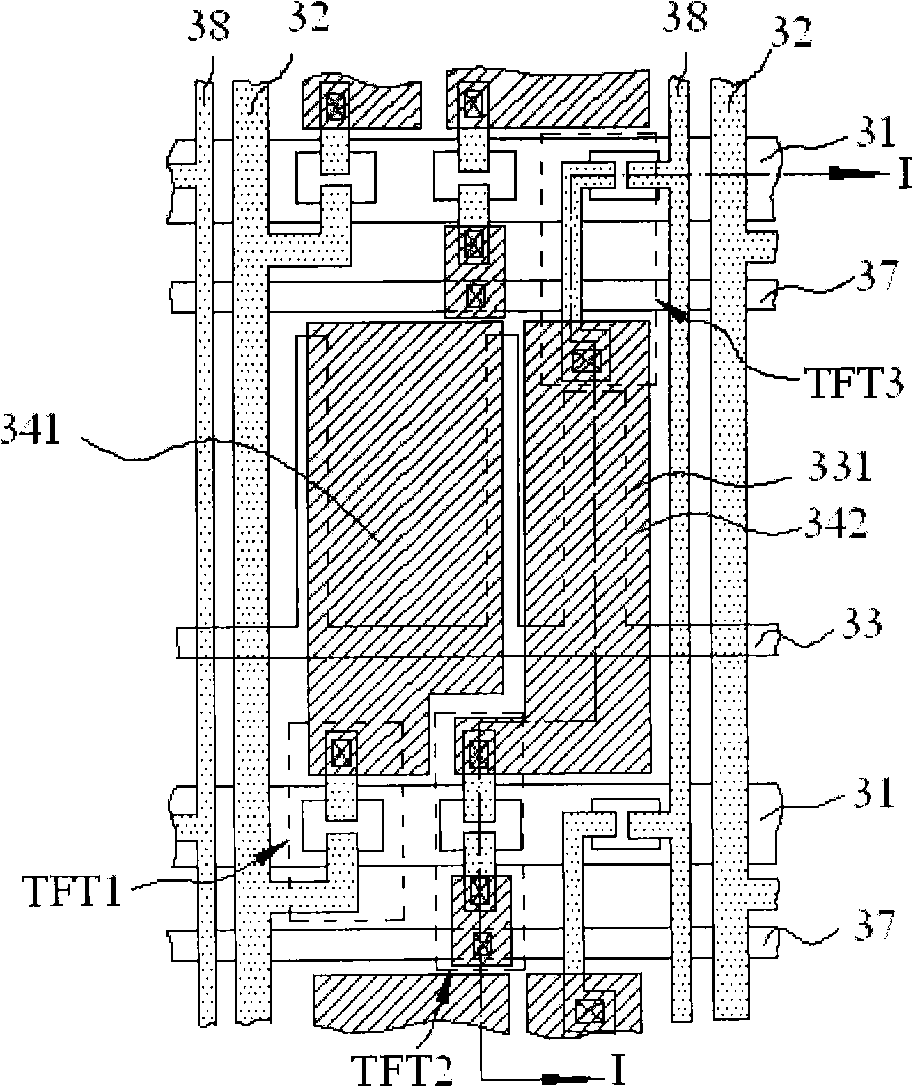
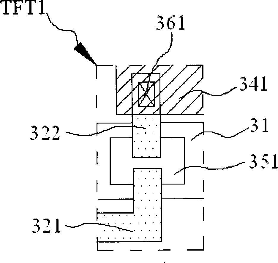
[0026] figure 1 A schematic diagram of the pixel structure of the first embodiment of the present invention is shown. For clarity, the color filter substrate is omitted from the figure. figure 1 Among them, 31 is a scan line, 32 is a data line, 33 is a storage capacitor electrode line, and 331 is an extension of the storage capacitor electrode line 33 . The scan line 31 and the data line 32 are vertically intersected to define a pixel area, and the pixel electrode 341 is formed in the pixel area, and the pixel electrode 341 and the storage capacitor electrode line 33 form a first storage capacitor Cst. The counter electrode on the substrate (refer to image 3 ) form a liquid crystal capacitor C1c. A first thin film transistor TFT1 is disposed at the intersection of the scan line 31 and the data line 32 .
[0027] ...
PUM
 Abstract
Description
Claims
Application Information


