Motherboard and its internal memory apparatus

A memory and memory chip technology, applied in information storage, static memory, digital memory information, etc., can solve the problems of lower system performance, increased design complexity of memory controller 201, signal transmission delay, etc., to achieve the effect of improving system performance

Active Publication Date: 2010-06-23
ASUSTEK COMPUTER INC
View PDF4 Cites 0 Cited by
  • Summary
  • Abstract
  • Description
  • Claims
  • Application Information

AI Technical Summary

Problems solved by technology

[0009] However, under the fly-by bus architecture formulated by JEDEC, because the address line signal and command line signal sent by the memory controller 201 are sequentially transmitted from the memory chip DDR3 SDRAM0 to the memory chip DDR3 SDRAM7 in a serial manner, So it will cause a delay in signal transmission
Also because of this, each memory chip DDR3 SDRAM0~DDR3 SDRAM7 receives the address line signal and command line signal sent by the memory controller 201 and starts working at a different time point, so the memory controller 201 has to wait for a while The action of reading or writing data to the memory chips DDR3 SDRAM0~DDR3 SDRAM7 can be completed after a delay time, so the system performance per unit time of the desktop computer will be reduced
[0010] In addition, because the memory controller 201 has to wait for a period of delay before completing the action of reading or writing data to the memory chips DDR3 SDRAM0-DDR3 SDRAM7, the memory controller 201 must independently control each memory chip. DDR3 SDRAM0~DDR3 SDRAM7 can read or write data, so the design complexity of the memory controller 201 will increase a lot

Method used


Image

  • Motherboard and its internal memory apparatus
  • Motherboard and its internal memory apparatus
  • Motherboard and its internal memory apparatus

Examples


Embodiment Construction

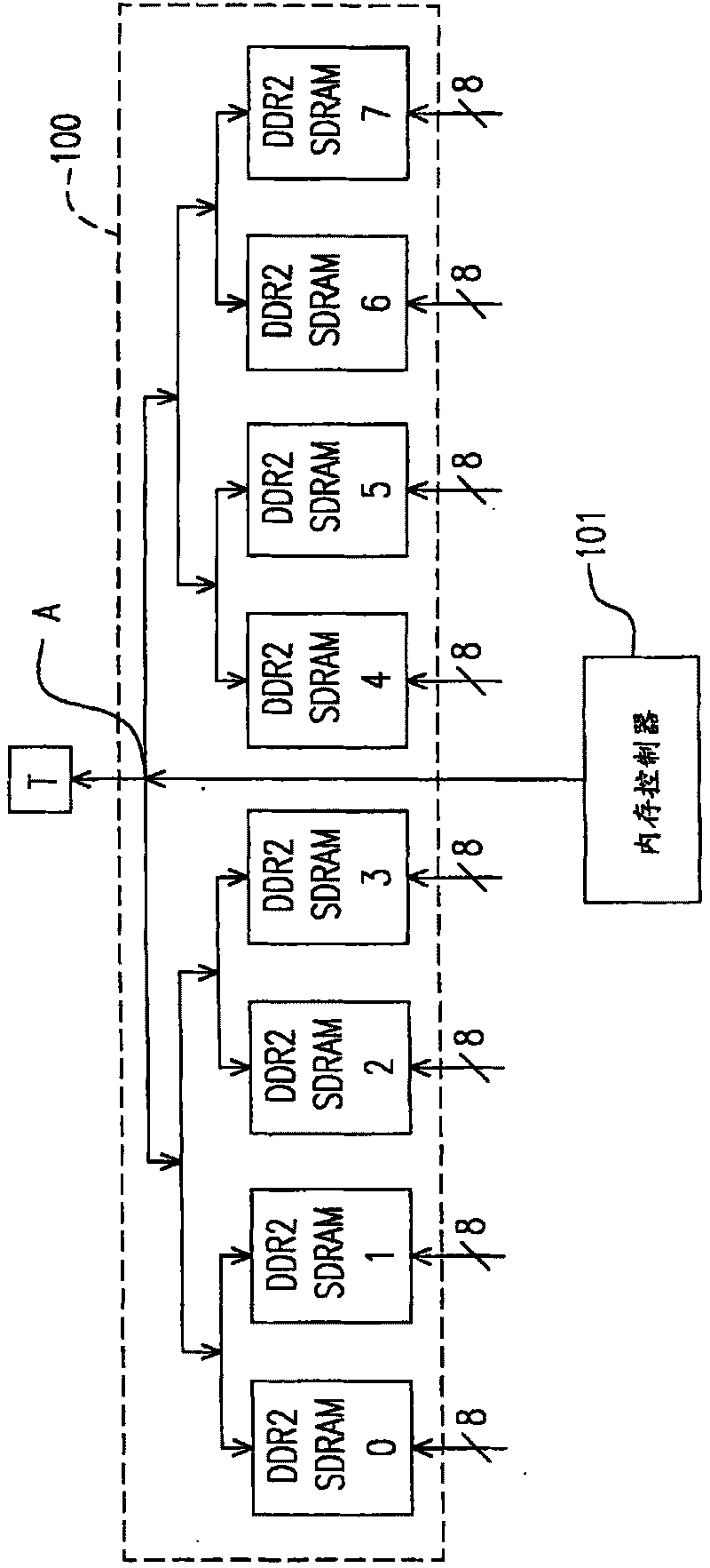
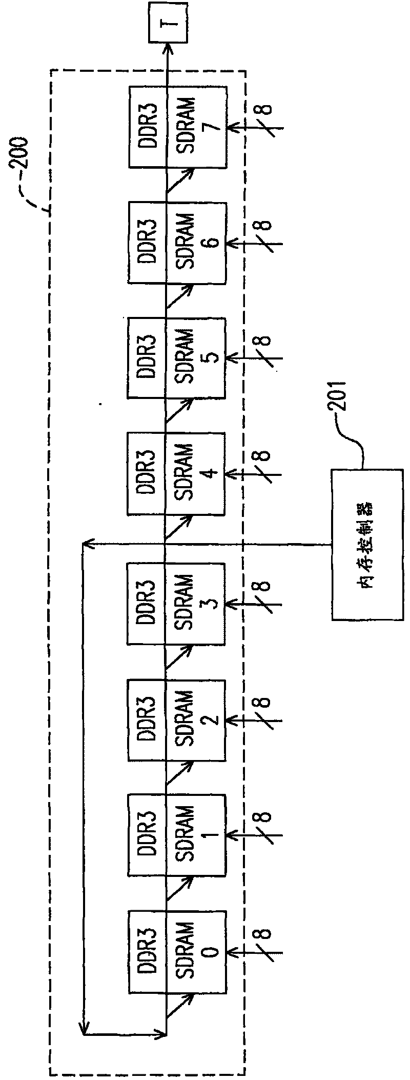
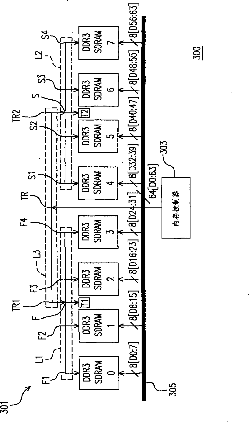
[0028] image 3 Shown is a motherboard 300 according to an embodiment of the present invention, which has a memory device 301 , and the memory device 301 is directly implanted on the motherboard 300 . In this embodiment, the memory device 301 includes a plurality of memory chips, such as 8 memory chips DDR3 SDRAM0-DDR3 SDRAM7, a first instruction / address line L1, a second instruction / address line L2, and a third instruction / address line L3 , a first terminator T1, a second terminator T2, a memory controller 303, and a data bus 305 composed of 64 data lines [D0:63]. Wherein, the memory chips DDR3 SDRAM0˜DDR3 SDRAM7 are divided into a first group of memory chips DDR3 SDRAM0˜DDR3 SDRAM3 and a second group of memory chips DDR3 SDRAM4˜DDR3 SDRAM7.

[0029] The first instruction / address line L1 has one first branch point F and four first branch points F1-F4, wherein the first branch point F is located at the center of the first instruction / address line L1, and each first branch poi...


PUM


Abstract

The present invention relates to a memory device, which can be directly arranged on any motherboard in the prior art which can support the third-generation dual-channel synchronous dynamic random access memory DDR3 SDRAM, so as to integrate the advantages of the fly-by bus bracket and the T-shaped branch bracket, which are prepared in the JEDEC. Therefore, the memory device can improve the systemefficiency of the table computer in unit time.

Description

technical field [0001] The present invention relates to a motherboard of a desktop computer and its memory device, and in particular to a motherboard and its memory capable of handling relatively high-frequency work and improving the system performance per unit time of the desktop computer. device. Background technique [0002] Generally speaking, the motherboards of today's desktop computers are often equipped with memory slots for users to insert memory modules (DIMMs). Such a framework is formulated by the Joint Electron Device Engineering Council (JEDEC). [0003] It is worth mentioning that JEDEC has formulated some recommended reference design architectures for PCunbuffered DIMMs for desktop computers. Among them, when the memory chip on the above-mentioned unbuffered memory module is the second generation of Double Data Rate Two Synchronous Dynamic Random Access Memory (DDR2 SDRAM), JEDEC recommends that the T branch topology ) to design, and when the memory chip o...

Claims


Application Information

Patent Timeline
Patent Type & Authority Patents(China)
IPC IPC(8): G11C5/00G11C8/12G06F13/00
Inventor 陈约志
Owner ASUSTEK COMPUTER INC
Why Eureka
Try Eureka