Method for judging wafer thinning, device structure and device and its manufacture method

A device structure and wafer technology, applied in the direction of manufacturing tools, grinding devices, surface polishing machine tools, etc., can solve problems such as delays in the grinding process and reduction in process output

Active Publication Date: 2009-01-07
TAIWAN SEMICON MFG CO LTD
View PDF1 Cites 23 Cited by
  • Summary
  • Abstract
  • Description
  • Claims
  • Application Information

AI Technical Summary

Problems solved by technology

Therefore, the grinding process will be delayed, resulting in a decrease in the overall process output

Method used


Image

  • Method for judging wafer thinning, device structure and device and its manufacture method
  • Method for judging wafer thinning, device structure and device and its manufacture method
  • Method for judging wafer thinning, device structure and device and its manufacture method

Examples


Embodiment Construction

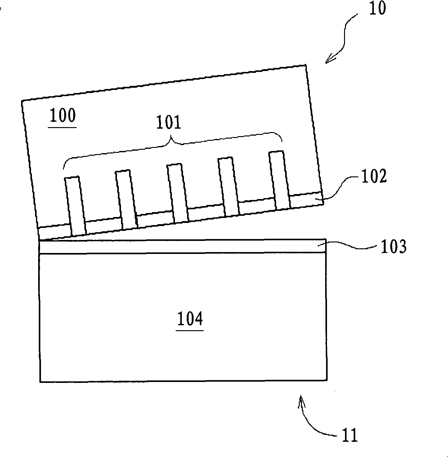
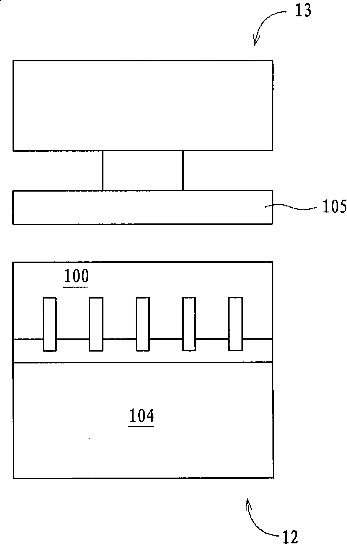
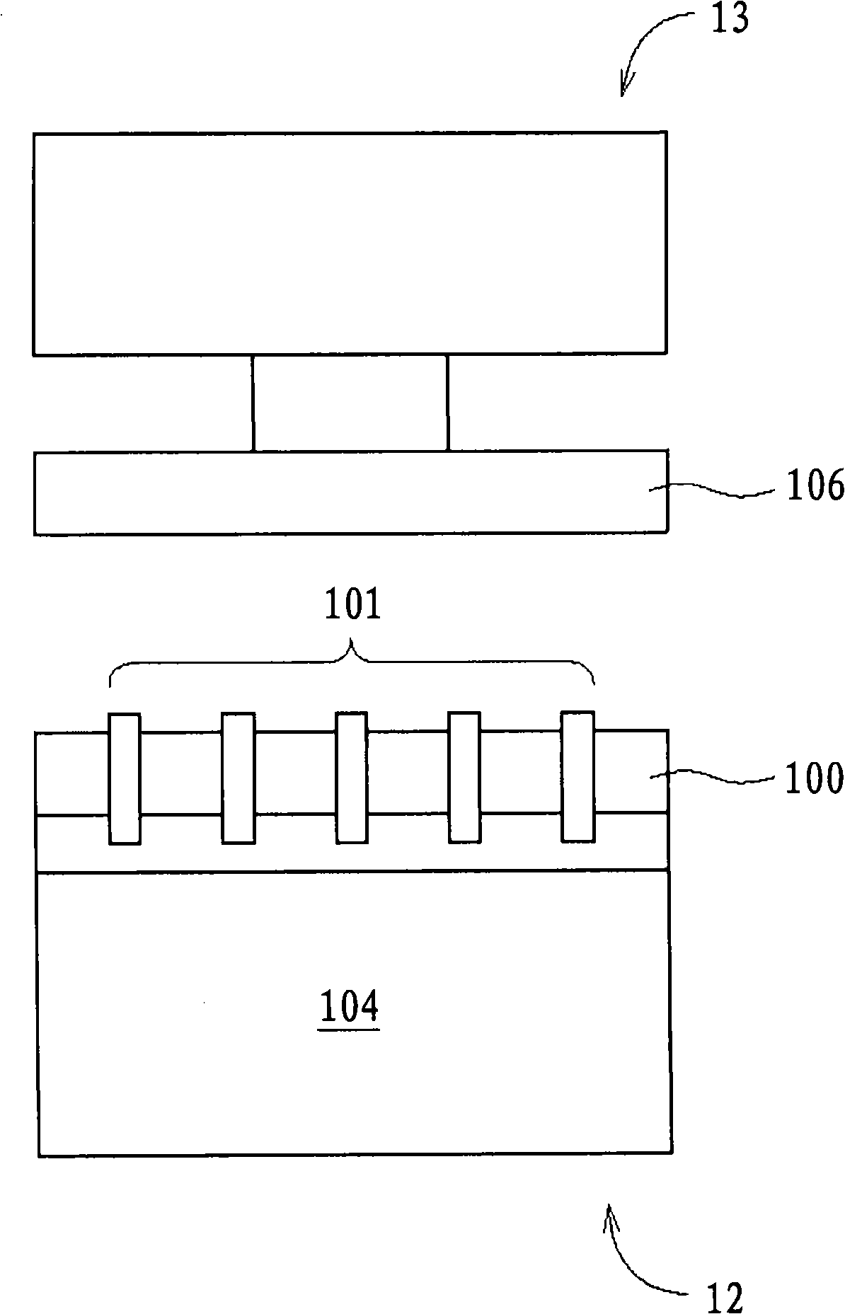
[0087] In order to further explain the technical means and effects adopted by the present invention to achieve the intended purpose of the invention, the method, device structure, mechanism and manufacturing thereof for judging wafer thinning proposed according to the present invention will be described below in conjunction with the accompanying drawings and preferred embodiments. The specific implementation, structure, method, steps, features and effects of the method are described in detail below.

[0088] The making and utilizing of preferred embodiments of the invention are discussed in detail below. It should be appreciated, however, that the present invention provides many applicable inventive concepts, which can be embodied in a wide variety of specific contexts. The specific embodiments discussed below are only used to illustrate the manufacture and utilization of the present invention in specific ways, and are not intended to limit the scope of the present invention. ...


PUM


Abstract

The invention relates to a method for judging wafer thinning, device structure, mechanism and its manufacture method. Basis material is ground and removed from semiconductor device; current change in grinding device is detected and responds to multiple first group of device structure exposing with basis material; the grinding and removing step responds to detected current change and stops; polishing step is performed to repairing surface, and extra basis material is continuously removed; other one or multiple groups of device structures with exposing material is monitored to judge extra amount of basis material to be removed; the other one or multiple groups of device structures is positioned inside semiconductor device at known depth other than the position depth of the first group structure.

Description

technical field [0001] The invention relates to a semiconductor wafer thinning, in particular to a method for judging wafer thinning, a device structure, a mechanism and a manufacturing method thereof. Background technique [0002] Regardless of whether in a bulk silicon semiconductor (bulk Si / semiconductor) wafer or a silicon-on-insulator (Si / semiconductor on insulator; SOI) package, the semiconductor wafer generally includes a first surface or a front surface on which an integrated circuit is formed, and at least The backside comprises a thickness of semiconductor material (eg, silicon, gallium arsenide, etc.). Before individual integrated circuit chips are diced and packaged, the backside of the wafer is generally thinned to remove unwanted semiconductor material. [0003] Depending on the type of semiconductor substrate (such as SOI vs. bulk silicon) or the process point of forming vias (before or after die attach), there are several different die attach and wafer thinn...

Claims


Application Information

Patent Timeline
Patent Type & Authority Applications(China)
IPC IPC(8): H01L21/00H01L21/66B24B49/02B24B49/10B24B37/04B24B29/00
CPCB24B37/013H01L2924/0002H01L22/26B24B7/228H01L21/76898H01L2924/00
Inventor 吴文进杨固峰张宏宾邱文智余振华
Owner TAIWAN SEMICON MFG CO LTD
Why Eureka
Try Eureka