Liquid crystal displays
A technology of liquid crystal display device and liquid crystal layer, which is applied in optics, instruments, nonlinear optics, etc., and can solve problems such as inability to be compensated
- Summary
- Abstract
- Description
- Claims
- Application Information
AI Technical Summary
Problems solved by technology
Method used
Image
Examples
no. 1 example
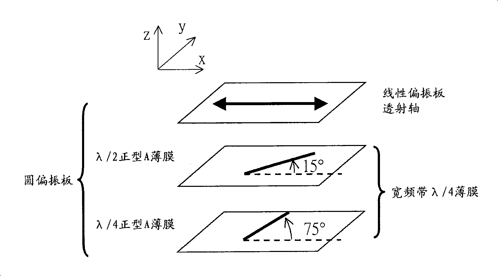
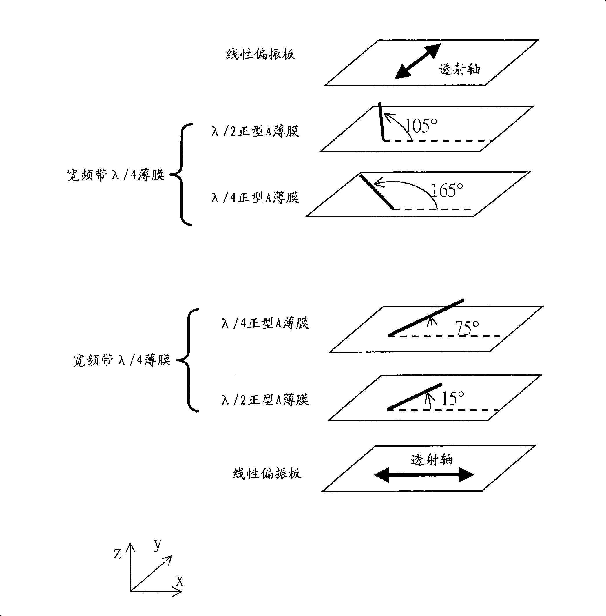
[0079] Please refer to Figure 3A , which is a cross-sectional view of the wide viewing angle and broadband circular polarizing plate of the first embodiment, and is constructed in a transflective LCD or used in a pure transmissive LCD. A liquid crystal layer 150, such as a vertically aligned liquid crystal cell, is sandwiched between a first glass substrate 155a and a second glass substrate 155b, wherein a thin film transistor (Thin Film Transistor, TFT) array is for example described in the following US Among the patents: U.S. Patents. 5,528,055 to Komori; 6,424,396 to Kim et al.; and 6,760,087. Each of the aforementioned patents is incorporated by reference. A TFT array can be formed on the bottom substrate 155a to provide driving voltage to regulate the liquid crystal layer therebetween.
[0080] Two stacked broadband circular polarizers 130a and 130b are placed between the liquid crystal layer and the two glass substrates, wherein the two circular polarizers compensate ...
no. 2 example
[0108] Please refer to Figure 9A , which shows a structural diagram of a second embodiment of the present invention. corresponds to Figure 3A The architecture, where each plate A is set to have opposite birefringence. The liquid crystal unit 250 is interposed between a first glass substrate 255a and a second glass substrate 255b, wherein a TFT array (not shown in Figure 9A ) can be formed on the bottom substrate 255a to provide a driving voltage to regulate the liquid crystal layer therebetween. Two stacked circular polarizing plates 230a and 230b are placed between the liquid crystal layer and the two glass substrates. The first circular polarizing plate 230a also includes a first linear polarizing plate 200a, a first half-wave plate 210a and a first quarter-wave plate 220a, and the second circular polarizing plate 230b also includes a second linear polarizing plate 200b , a second half-wave plate 210b and a second quarter-wave plate 220b. Please refer to Figure 9B ...
no. 3 example
[0113] Please refer to Figure 12A , which is a structural diagram of a third embodiment of the present invention. In addition, in the structure of circular polarizing plates suitable for wide viewing angles and wide frequency bands of transflective LCDs proposed in this example, although the half-wave plates and quarter-wave plates of each circular polarizing plate have the same type ( For example: both are positive A-plates or negative-type plates), but the half-wave plates or quarter-wave plates corresponding to different circular polarizing plates have opposite types. At Figure 12A Among them, the first circular polarizing plate 330a with broadband and wide viewing angle characteristics is formed by a first linear polarizing plate 300a, a first half-wave plate 310a, and a first quarter-wave plate 320a. The half-wave plates and quarter-wave plates of the first circular polarizing plate are made of positive type A plates, wherein the transmission axis 301a of the first li...
PUM
| Property | Measurement | Unit |
|---|---|---|
| refractive index | aaaaa | aaaaa |
| refractive index | aaaaa | aaaaa |
Abstract
Description
Claims
Application Information


