

Laminated capacitor
A multi-layer capacitor and stacking technology, applied in the direction of multi-layer capacitors, fixed capacitor electrodes, multiple fixed capacitors, etc., can solve the problems of easy to increase in size, can not adapt to the high speed of CPU, etc., to reduce ESL and suppress power supply voltage the effect of changes
- Summary
- Abstract
- Description
- Claims
- Application Information
AI Technical Summary
Problems solved by technology
Method used
Image

Examples
no. 1 Embodiment approach
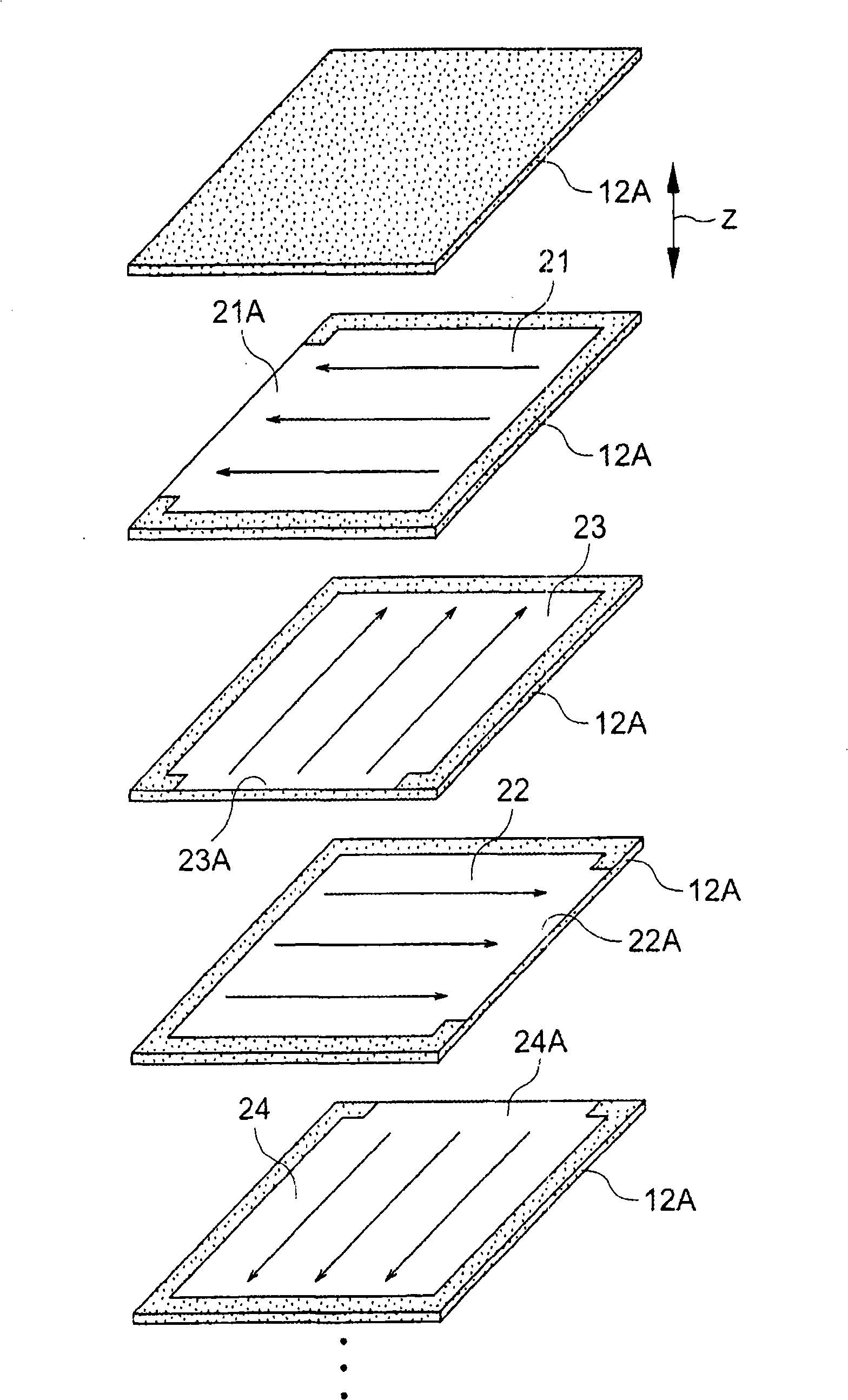
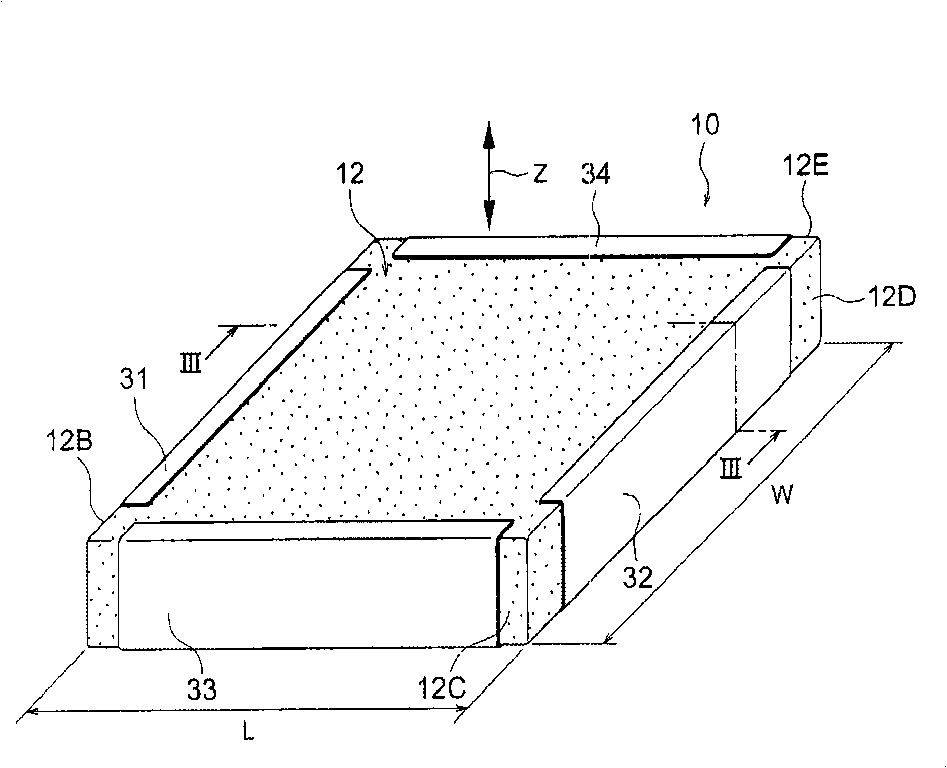
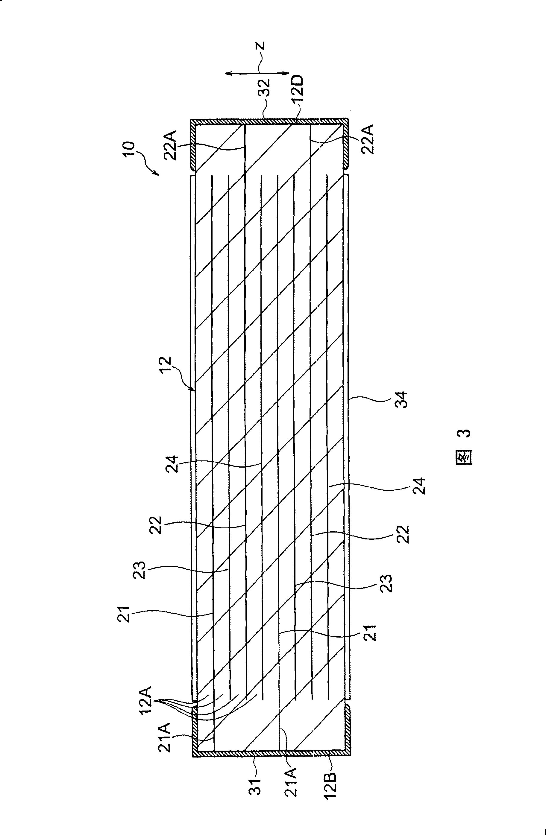
[0074] Figure 1 to Figure 4 A multilayer ceramic capacitor (hereinafter referred to as a multilayer capacitor) 10 of the present embodiment is shown. As shown in these figures, this multilayer capacitor 10 has a rectangular parallelepiped sintered body obtained by firing a laminated body, that is, a dielectric element 12 as its main part. It is obtained by laminating ceramic green sheets. In the dielectric body 12, first inner conductors 21, second inner conductors 23, first inner conductors 22, and second inner conductors 24 each formed in a substantially square (or rectangular) shape are arranged in order from the top. Ceramic layers 12A are arranged between the respective internal conductors.
[0075] In this embodiment, fired ceramic layers 12A serving as dielectric sheets are respectively sandwiched, and four types of internal conductors 21 , 23 , 22 , and 24 are sequentially arranged in the dielectric body 12 . On the lower side of the inner conductor 24, as shown in...
no. 2 Embodiment approach
[0098] Second, according to Figure 5 A second embodiment of the multilayer capacitor of the present invention will be described with FIG. 6 . In addition, the same symbol is added to the same member as what was already demonstrated in 1st Embodiment, and repeated description is abbreviate|omitted.
[0099] In the first embodiment described above, the internal conductors are individually formed on the same plane. On the other hand, the internal conductor of this embodiment is such as Figure 5 As shown in FIG. 6, the inner conductors located in the same plane are divided so as to extend side by side with each other. exist Figure 5 The first internal conductors 21 of the uppermost stacked layer are alternately drawn out to the two opposite sides 12B, 12D of the dielectric unit 12 (shown in figure 2 ) of a plurality of (two in this embodiment) divided conductors 41, 42.
[0100] The first inner conductor 22 paired with the first inner conductor 21 is also divided so as to...
no. 3 Embodiment approach
[0107] Second, according to Figure 7 A third embodiment of the multilayer capacitor of the present invention will be described. In addition, the same symbol is added to the same member as what was already demonstrated in 1st Embodiment, and repeated description is abbreviate|omitted.
[0108] In this embodiment, if Figure 7 As shown, the first internal conductor 21 is alternately drawn out to two opposite side surfaces 12B, 12D of the dielectric unit 12 by extending side by side with each other (shown in figure 2 ) of multiple (three in this form) segmented conductors 51, 52, 53.
[0109] In addition, the first inner conductor 22 is similarly divided and drawn out to two opposite side surfaces 12B, 12D of the dielectric body 12 (shown in figure 2 ) of multiple (three in this embodiment) segmented conductors 54, 55, 56. These split conductors 54 , 55 , 56 overlap with split conductors 51 , 52 , 53 when viewed from a planar direction, but the overlapped split conductors ...
PUM
 Abstract
Description
Claims
Application Information