
Printed circuit board and manufacturing method thereof

A technology for printed circuit boards and circuit patterns, applied in the directions of printed circuit manufacturing, printed circuits, printed circuits, etc., can solve the problems of contamination of mounting components, weakened adhesion of pads 104, insufficient adhesion, etc., to enhance adhesion and improve heat release. performance, enhanced connectivity

Active Publication Date: 2009-01-28
SAMSUNG ELECTRO MECHANICS CO LTD
View PDF1 Cites 10 Cited by
  • Summary
  • Abstract
  • Description
  • Claims
  • Application Information

AI Technical Summary

Problems solved by technology

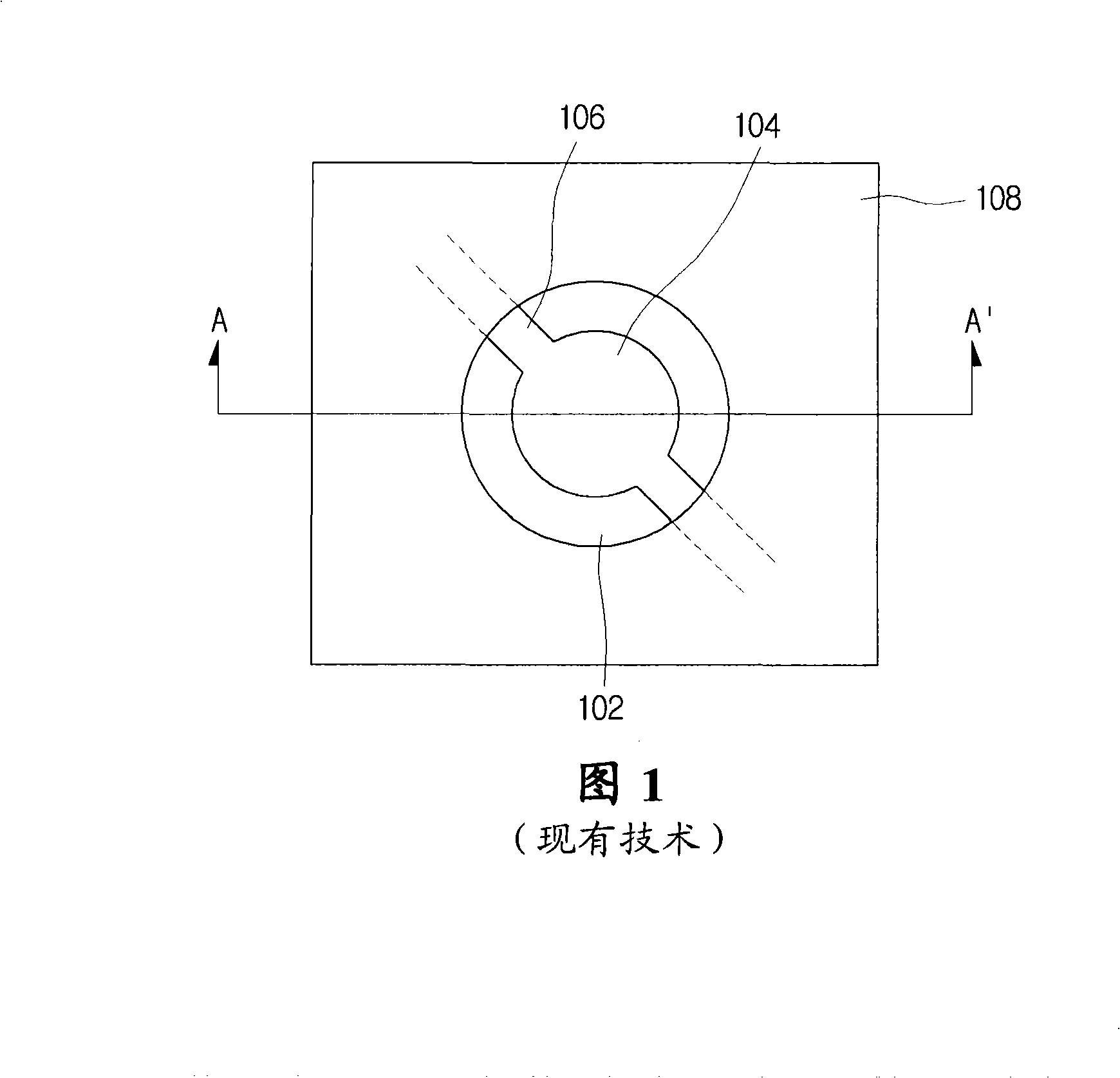
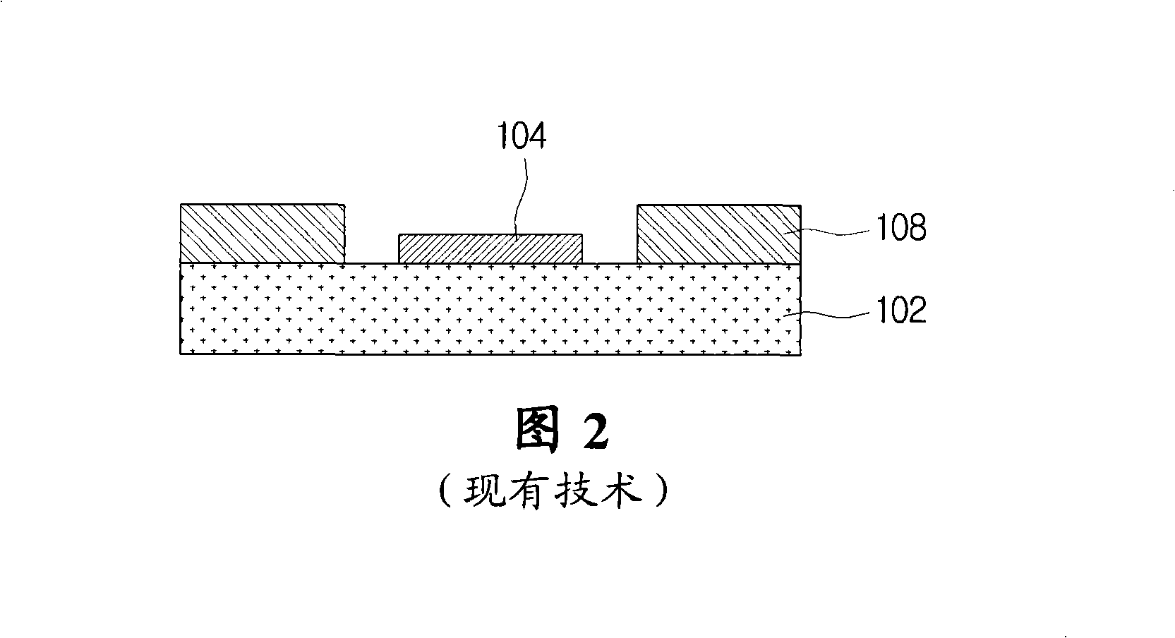
Although the NSMD structure provides high-reliability contact and ultra-high heat release performance when mounting components, because the pad 104 is completely exposed to the outside, when part of the insulating layer 102 and the pad 104 are completely exposed to the external environment, there is a problem of mounting Risk of component contamination before
Also, due to the small attachment area, there is a risk that the adhesion of the pad 104 will weaken
[0008] Specifically, with the current trend toward miniaturization of the circuit pattern 106, the attachment area between the pad 104 and the insulating layer 102 becomes even smaller, so insufficient adhesion may occur, causing the pad 104 to peel off from the insulating layer 102.

Method used


Image

  • Printed circuit board and manufacturing method thereof
  • Printed circuit board and manufacturing method thereof
  • Printed circuit board and manufacturing method thereof

Examples


Embodiment Construction

[0027] As the invention contemplates various changes and embodiments, specific embodiments will be illustrated in the drawings and described in detail in the written description. However, this is not intended to limit the present invention to specific embodiments, and it should be understood that all changes, equivalent replacements, and replacements that do not depart from the spirit and technical scope of the present invention are included in the present invention. In describing the present invention, some detailed descriptions of related arts are omitted when it is considered that they may unnecessarily obscure the gist of the invention.

[0028] Although terms such as 'first', 'second', etc. may be used to describe various elements, these elements are not limited to the above terms. The above terms are only used to distinguish one element from another.

[0029] The terms used in the present invention are used to describe specific embodiments only, and are not intended to ...


PUM


Abstract

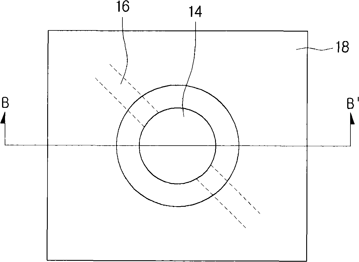
A printed circuit board and a method of manufacturing the printed circuit board are disclosed. A printed circuit board, which includes an insulation layer, a circuit pattern formed on a surface of the insulation layer that includes at least one pad, and a solder resist which covers the circuit pattern, and in which an opening is formed that exposes a portion of a side and a surface of the pad, can ensure a sufficient amount of attachment area for the pads and the solder resist, to strengthen the adhesion of the pads. Also, the adhesion can be increased between the electronic components and the printed circuit board, and heat release characteristics can be improved.

Description

[0001] Related Application Cross Reference [0002] This application claims the benefit of Korean Patent Application No. 10-2007-0075185 filed with the Korean Intellectual Property Office on Jul. 26, 2007, the disclosure of which is hereby incorporated by reference in its entirety. technical field [0003] The present invention relates to a printed circuit board and a method of manufacturing the printed circuit board. Background technique [0004] With the development of the electronics industry, portable electronic products, including those used in mobile phones and DMB (Digital Multimedia Broadcasting), are becoming smaller and more functional, resulting in the demand for miniaturized, highly integrated, multifunctional The demand for advanced and high-performance electronic components. With the high integration of electronic components, the number of I / O (input / output) continues to increase, so an increased number of pads on the printed circuit board is required for moun...

Claims


Application Information

Patent Timeline
Patent Type & Authority Applications(China)
IPC IPC(8): H05K1/02H05K3/28
CPCY10T29/49165H05K2203/0594H05K2201/09845H05K3/0032H05K3/3452H05K1/02
Inventor 赵贞禹李宗辰曹淳镇李用德刘己荣李宇永金镇宽金钟涌田东柱
Owner SAMSUNG ELECTRO MECHANICS CO LTD
Learn More