Manufacturing method of green light LED

A technology of light-emitting diodes and manufacturing methods, which can be applied to semiconductor devices, electrical components, circuits, etc., and can solve problems such as poor antistatic ability and low external quantum efficiency

Active Publication Date: 2009-02-04
EPILIGHT TECH +2
View PDF0 Cites 47 Cited by
  • Summary
  • Abstract
  • Description
  • Claims
  • Application Information

AI Technical Summary

Problems solved by technology

[0003] In recent years, the external quantum efficiency of GaN-based blue LEDs has been greatly improved, reaching 45% (see: Appl. Phys. Lett 89, 071109), but the external quantum efficiency of green light-emitting diodes is much lower than that of GaN-based blue LEDs ( See: Appl.Phys.Lett 86, 101903, etc.), green light-emitting diodes require high-quality high-In composition InxGa1-xN / GaN quantum wells (x≥15%), but due to the high-In composition InGaN material is prone to The phase separation of In, and the interface of InxGaN / GaN multi-quantum wells are prone to produce a large number of V-type defects. The above are the main reasons for the low external quantum efficiency and poor antistatic ability of green LEDs.

Method used


Image

  • Manufacturing method of green light LED
  • Manufacturing method of green light LED

Examples


Embodiment 1

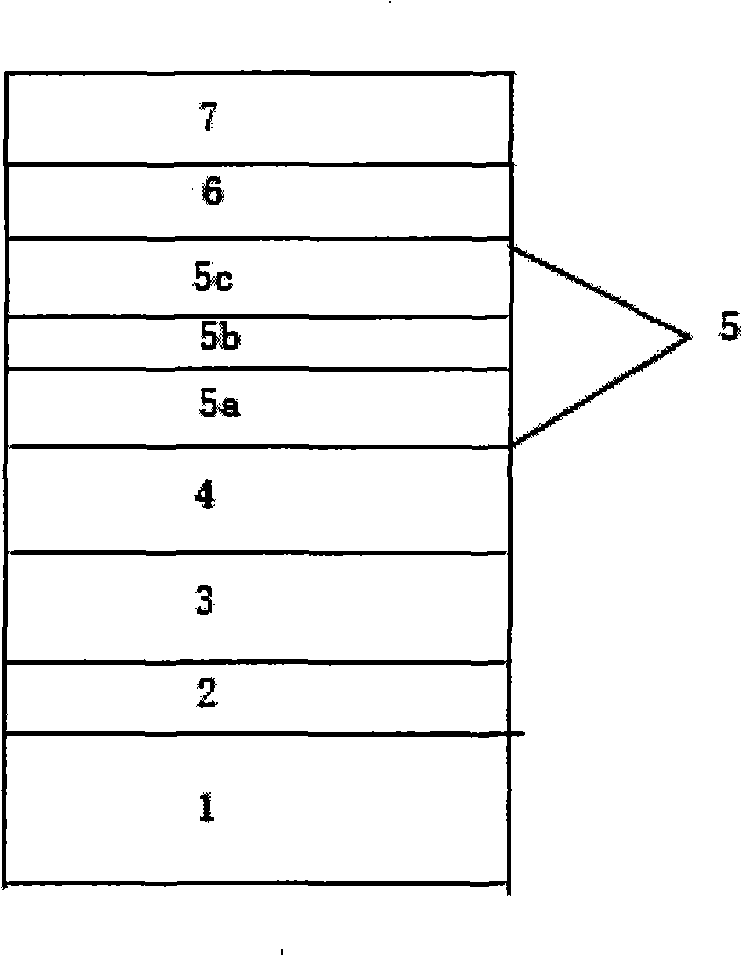
[0022] Using MOCVD equipment to epitaxially grow high-brightness green light-emitting diodes, the substrate used is (001) sapphire. like figure 1 As shown, firstly, the sapphire substrate 1 is heated to 1200°C in the MOCVD reaction chamber, treated under H2 for 5 minutes, and then the temperature is lowered to 500-600°C to grow the GaN nucleation layer 2 with a thickness of about 30nm; then the temperature is raised to 1160°C , H2 as carrier gas, epitaxially grown a 4-micron-thick GaN buffer layer at a growth rate of 3.0 microns / hour, including a 0.5-micron-thick unintentionally doped GaN layer 3 and a 3.5-micron-thick Si-doped n-type GaN buffer layer 4. The doping concentration of silicon is 5×10 17 cm -3 up to 5×10 19 cm -3 between; then lower the temperature to 650-750°C, switch the carrier gas to N2, and grow 5 In on the buffer layer 0.2 Ga 0.8 N(2.5nm) / In 0.8 Ga 0.2 N(0.5nm) / GaN(10nm), where the molar flow of TEGa is 0.1×10 -5 mol / min to 1.5×10 -5 mol / min, the m...

Embodiment 2

[0024] Using MOCVD equipment to epitaxially grow high-brightness green light-emitting diodes, the substrate used is (001) sapphire. like figure 1 As shown, firstly, the sapphire substrate 1 is heated to 1200°C in the MOCVD reaction chamber, treated under H2 for 5 minutes, and then the temperature is lowered to 500-600°C to grow the GaN nucleation layer 2 with a thickness of about 30nm; then the temperature is raised to 1160°C , H2 as carrier gas, epitaxially grown a 4-micron-thick GaN buffer layer at a growth rate of 3.0 microns / hour, including a 0.5-micron-thick unintentionally doped GaN layer 3 and a 3.5-micron-thick Si-doped n-type GaN buffer layer 4. The doping concentration of silicon is 5×10 17 cm -3 up to 5×10 19 cm -3 between; then lower the temperature to 650-750°C, switch the carrier gas to N2, and grow 5 In on the buffer layer 0.2 Ga 0.8 N(2.5nm) / Al 0.8 Ga 0.2 N(0.5nm) / GaN(10nm), where the molar flow of TEGa is 0.1×10 -5 mol / min to 1.5×10 -5 mol / min, the m...


PUM


Abstract

The invention relates to a method for fabricating a green LED, which is mainly characterized in that through the introduction of an insert layer into an epitaxial growth InGaN/GaN quanta well, V type defects between the InGaN and the GaN is reduced and In precipitation is reduced; thus, the green LED with high brightness and strong antistatic ability can be obtained. With the introduction of the insert layer, the brightness of a 300micronx300micron green LED chip at 520nm under 20mA is improved from 100mcd to 250mcd and the antistatic ability of the chip is increased from HBM 500V (human-body model) to HBM 4000V.

Description

technical field [0001] The invention relates to a metal organic vapor deposition (MOCVD) epitaxial growth method of a III-V nitride material based on gallium nitride (GaN), in particular to a manufacturing method of a green light emitting diode. Background technique [0002] GaN-based III-V nitrides are important direct-bandgap wide-bandgap semiconductor materials. GaN-based materials have excellent material mechanical and chemical properties, excellent photoelectric properties, and their bandgap ranges from 0.7eV (InN) to 6.2eV (AlN) at room temperature. Deep ultraviolet, GaN-based materials have a wide range of application backgrounds in the field of optoelectronic devices such as blue light, green light, purple light and white light diodes. [0003] In recent years, the external quantum efficiency of GaN-based blue LEDs has been greatly improved, reaching 45% (see: Appl. Phys. Lett 89, 071109), but the external quantum efficiency of green light-emitting diodes is much lo...

Claims


Application Information

Patent Timeline
Patent Type & Authority Applications(China)
IPC IPC(8): H01L33/00
Inventor 潘尧波郝茂盛颜建锋周健华张国义
Owner EPILIGHT TECH
Why Eureka
Try Eureka