A kind of LED epitaxial structure and preparation method thereof and LED chip

An epitaxial structure, multiple quantum well technology, applied in semiconductor devices, electrical components, circuits, etc., can solve problems such as low quantum efficiency, and achieve the effects of improving microstructure, improving crystal quality, and low defect density

Active Publication Date: 2022-07-26
CHONGQING KONKA PHOTOELECTRIC TECH RES INST CO LTD
View PDF13 Cites 0 Cited by
  • Summary
  • Abstract
  • Description
  • Claims
  • Application Information

AI Technical Summary

Problems solved by technology

[0004] In view of the above deficiencies in the prior art, the purpose of the present invention is to provide an LED epitaxial structure and its preparation method and LED chip, aiming to solve the problem of low quantum efficiency in the existing high In composition LED

Method used


Image

  • A kind of LED epitaxial structure and preparation method thereof and LED chip
  • A kind of LED epitaxial structure and preparation method thereof and LED chip
  • A kind of LED epitaxial structure and preparation method thereof and LED chip

Examples


Embodiment Construction

[0031] The present invention provides an LED epitaxial structure, a preparation method thereof, and an LED chip. In order to make the purpose, technical solutions and effects of the present invention clearer and clearer, the present invention is further described below in detail. It should be understood that the specific embodiments described herein are only used to explain the present invention, but not to limit the present invention.

[0032] Unless otherwise defined, all technical and scientific terms used herein have the same meaning as commonly understood by one of ordinary skill in the art to which this invention belongs. The terms used herein in the description of the present invention are for the purpose of describing specific embodiments only, and are not intended to limit the present invention.

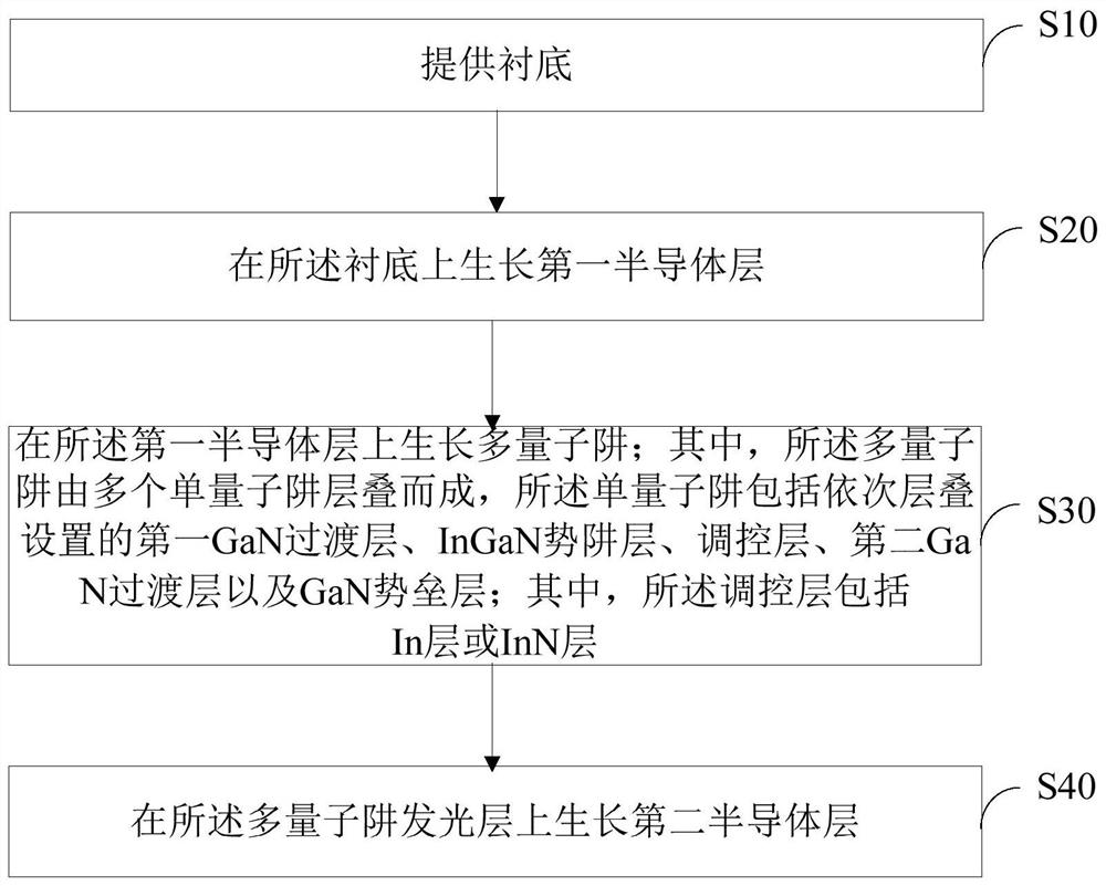
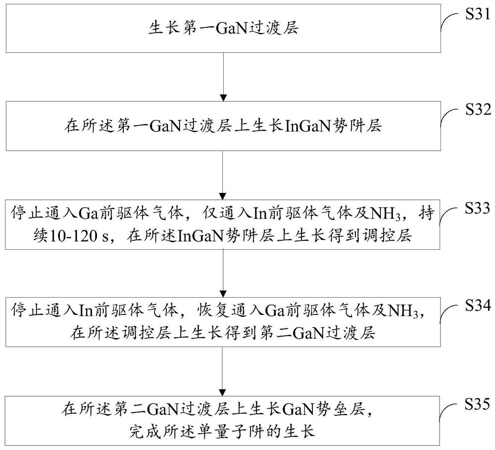
[0033] Embodiments of the present invention provide a method for fabricating an LED epitaxial structure, such as figure 1 As shown, the method includes:

[0034] S10, prov...


PUM

PropertyMeasurementUnit
thicknessaaaaaaaaaa
thicknessaaaaaaaaaa
thicknessaaaaaaaaaa

Abstract

The invention discloses an LED epitaxial structure, a preparation method thereof, and an LED chip. The LED epitaxial structure includes a first semiconductor layer, a multi-quantum well and a second semiconductor layer that are stacked in sequence, and the multi-quantum well is formed by stacking a plurality of single quantum wells, wherein the single quantum well includes stacking and stacking in sequence. The first GaN transition layer, the InGaN potential well layer, the regulation layer, the second GaN transition layer and the GaN barrier layer; wherein, the regulation layer includes an In layer or an InN layer. The structure of the invention can effectively improve the interface quality of the multiple quantum wells, suppress the segregation of In, and reduce the density of point defects; make the interface of the well barrier layer steeper and smoother, and reduce the V-shaped defect density in the multiple quantum wells, so that the non-radiative The recombination rate is reduced; the threading dislocations in the multiple quantum wells are annihilated at the interface, and the threading dislocation density is reduced, thereby reducing the leakage current and improving the luminous efficiency of the LED epitaxial structure.

Description

technical field [0001] The invention relates to the technical field of semiconductors, and in particular, to an epitaxial structure of a light-emitting diode (Light-Emitting Diode, LED for short), a preparation method thereof, and an LED chip. Background technique [0002] In recent years, GaN (gallium nitride)-based LEDs have attracted widespread attention due to their high reliability, high cost performance and high efficiency, and have been used in various industries; and InGaN (indium gallium nitride) materials are controlled by composition, and their The energy band gap can be continuously adjusted in the range of 0.7eV to 6.2eV, so the light emission of LEDs with InGaN / GaN multiple quantum well structures covers the entire visible light range, and has huge advantages in Mini / Micro LED (micro / mini LED) displays. application prospects. However, current LEDs with high In composition still face serious problems of low internal quantum efficiency, mainly due to two reasons...

Claims


Application Information

Patent Timeline
Patent Type & Authority Patents(China)
IPC IPC(8): H01L33/06H01L33/32H01L33/00
CPCH01L33/06H01L33/0075H01L33/32
Inventor 李兵兵黄国栋黄嘉宏林雅雯杨顺贵
Owner CHONGQING KONKA PHOTOELECTRIC TECH RES INST CO LTD
Why Eureka
Try Eureka