Circuit board leveling apparatus and method for leveling circuit board

A technology for leveling devices and circuit boards, applied in the directions of printed circuits, printed circuit manufacturing, electrical components, etc., can solve problems such as the inability to reduce warpage of circuit boards

Inactive Publication Date: 2010-11-17
AVARY HLDG (SHENZHEN) CO LTD +1
View PDF3 Cites 2 Cited by
  • Summary
  • Abstract
  • Description
  • Claims
  • Application Information

AI Technical Summary

Problems solved by technology

However, the simulation of the warpage of the circuit board can only optimize the wiring and assembly design of the circuit board, so that the design and manufacture of the circuit board adopts a process with a small warpage as much as possible, which cannot produce beneficial, Improved effect of reducing warpage

Method used


Image

  • Circuit board leveling apparatus and method for leveling circuit board
  • Circuit board leveling apparatus and method for leveling circuit board
  • Circuit board leveling apparatus and method for leveling circuit board

Examples


Embodiment Construction

[0017] The circuit board leveling device and the method for leveling the circuit board in the embodiment of the technical solution will be further described in detail below with reference to the accompanying drawings.

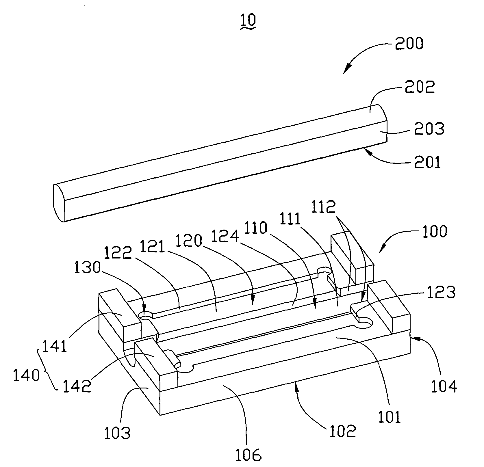
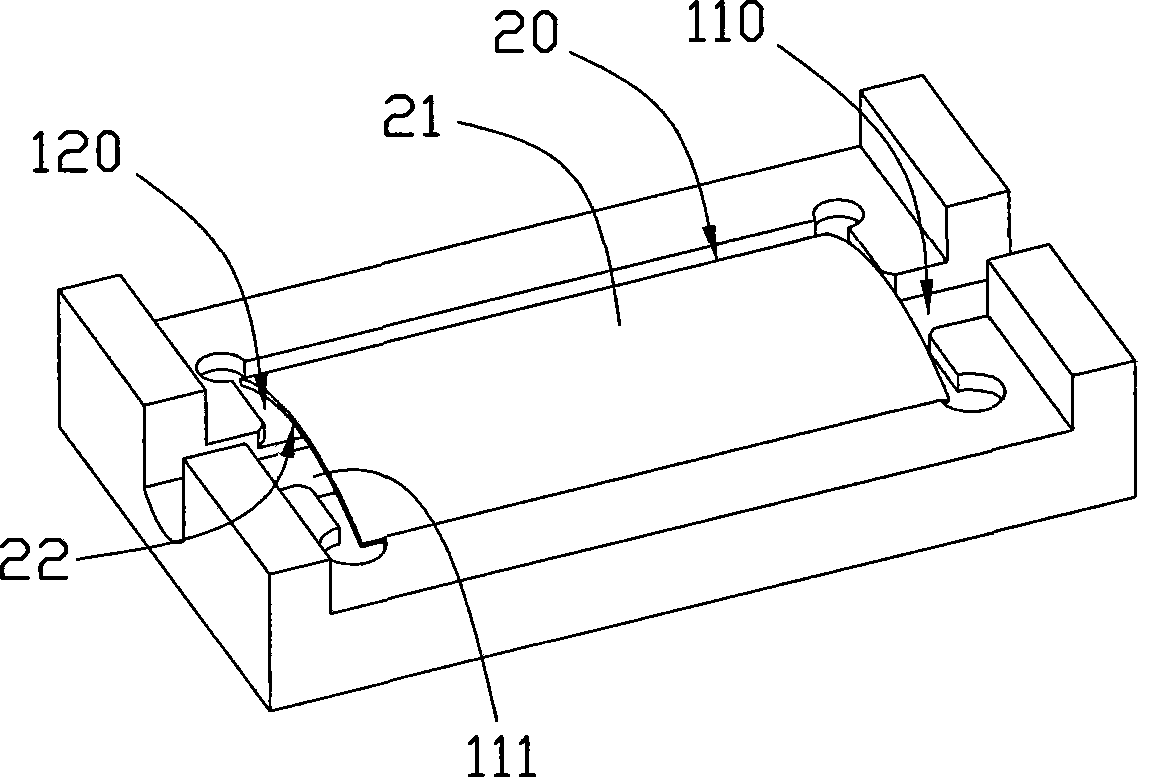
[0018] see figure 1 , The circuit board leveling device 10 in the embodiment of the technical solution includes a carrying jig 100 and a pressing element 200 . The carrying jig 100 is used to carry the circuit board to be leveled, and the pressing element 200 is used to press the circuit board to be leveled between the carrying jig 100 and the pressing element 200 to perform the circuit Plate leveling.

[0019] The carrying fixture 100 is in the shape of a cuboid and includes a first top surface 101 , a first bottom surface 102 , a first side surface 103 , a second side surface 104 , a third side surface 105 and a fourth side surface 106 . The first top surface 101 and the first bottom surface 102 are opposite and parallel to each other. The first side 103 a...


PUM


Abstract

The invention provides a circuit board flatting device, which includes a bearing tool and a pressing component. The bearing tool is provided with a first bearing plane, and the first bearing plane is concave; the pressing component is provided with a pressing plane, and the pressing plane and the first bearing plane are convexity. The technical proposal also provides a method of utilizing the circuit board flatting device to flat the circuit board. The circuit board flatting device and the method of flatting circuit board in the technical proposal can effectively flat circuit boards with certain warping.

Description

technical field [0001] The invention relates to the field of circuit board manufacturing, in particular to a circuit board leveling device and a circuit board leveling method. Background technique [0002] In the information, communication and consumer electronics industries, circuit boards are an indispensable and basic component of all electronic information products. The circuit board can realize the electrical connection of various electronic components, so that each electronic component can cooperate to process and transmit signals. [0003] In general, the circuit board should have good flatness, that is, the warpage of the circuit board should be reduced as much as possible, so as to facilitate the smooth progress of the automatic insertion and surface mount process of electronic components, and ensure the insertion and safety of electronic components. Mounting yield. The IPC-6012 test standard requires that the maximum warpage of surface-mounted circuit boards shou...

Claims


Application Information

Patent Timeline
Patent Type & Authority Patents(China)
IPC IPC(8): H05K3/00
Inventor 叶佐鸿杨智康张宏毅
Owner AVARY HLDG (SHENZHEN) CO LTD
Why Eureka
Try Eureka