Beam transforming element, illumination optical apparatus, exposure apparatus, and exposure method

An illuminating device and optical technology, applied in the direction of photolithography process exposure device, optical element, microlithography exposure equipment, etc., can solve the problems of light loss, low light throughput of exposure device, etc., and achieve high productivity and suppress the effect of light loss.

Inactive Publication Date: 2009-02-18
NIKON CORP
View PDF3 Cites 2 Cited by
  • Summary
  • Abstract
  • Description
  • Claims
  • Application Information

AI Technical Summary

Problems solved by technology

As a result, in the conventional technology, a large amount of light loss occurs at the aperture aperture, causing an unsuitable phenomenon that the light flux of the exposure device is reduced.

Method used


Image

  • Beam transforming element, illumination optical apparatus, exposure apparatus, and exposure method
  • Beam transforming element, illumination optical apparatus, exposure apparatus, and exposure method
  • Beam transforming element, illumination optical apparatus, exposure apparatus, and exposure method

Examples


Embodiment Construction

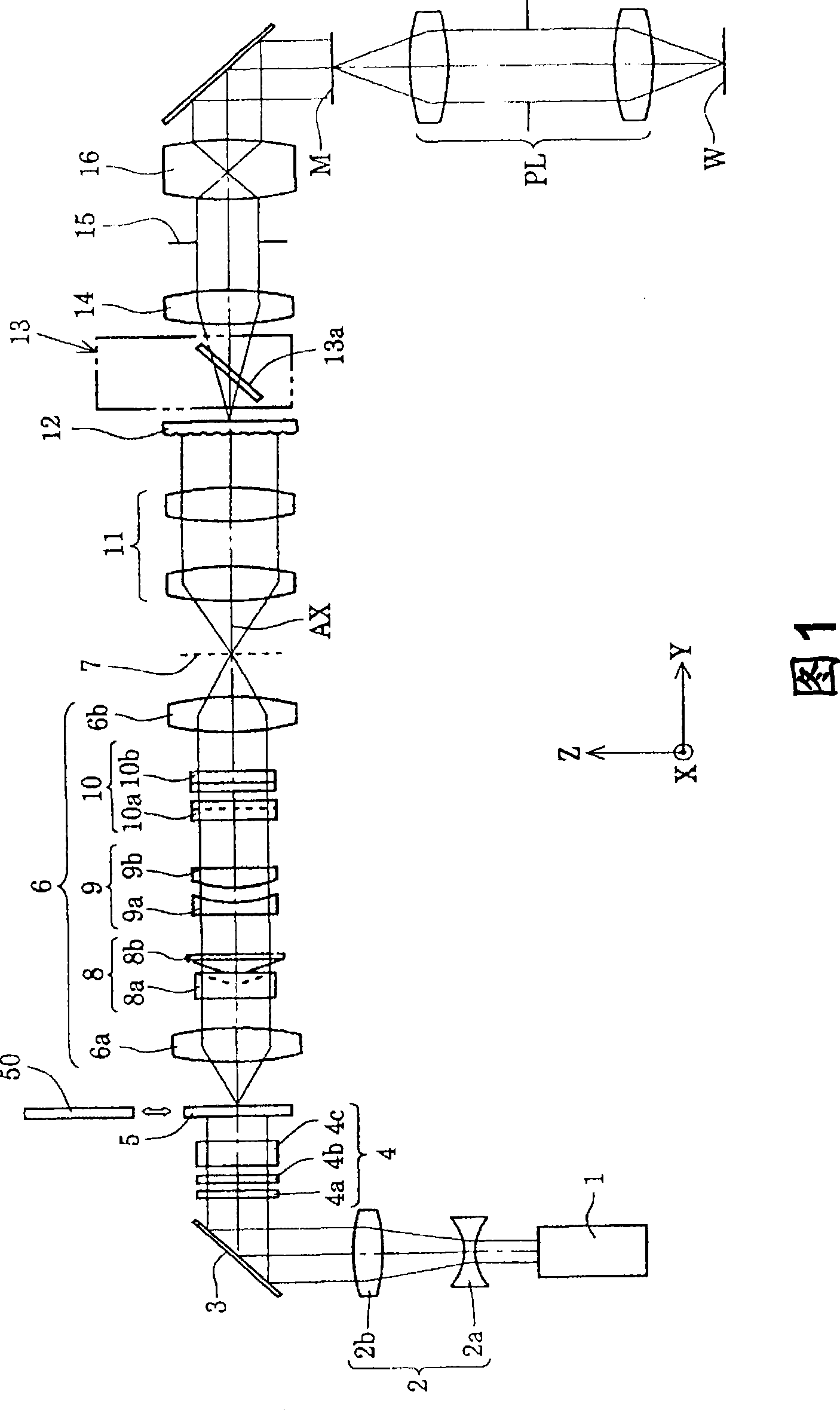
[0070] Hereinafter, embodiments of the present invention will be described based on the attached drawings.

[0071] FIG. 1 is a schematic diagram showing the configuration of an exposure apparatus equipped with an optical illumination device according to an embodiment of the present invention. In FIG. 1, the normal direction of the wafer W as the photosensitive substrate is set as the Z axis, and the direction parallel to the paper surface of FIG. 1 in the plane of the wafer W is the Y axis. The vertical direction of the paper surface of Fig. 1 is the X axis. The exposure apparatus of this embodiment is provided with a light source 1 for supplying light for exposure (illumination light).

[0072] As the light source 1 , for example, a KrF excimer laser (Excimer Laser) light source that supplies light with a wavelength of 248 nm or an ArF excimer laser light source that supplies light with a wavelength of 193 nm can be used. The approximately parallel light beam emitted from ...


PUM


Abstract

A lighting optical device capable of forming a bracelet-form lighting pupil distribution in a peripherally-polarized state with a light quantity loss satisfactorily controlled, the device comprising a light flux conversion element (50) for forming a bracelet-form light intensity distribution on a specified surface based on an incident light flux. The light flux conversion element comprises a first basic element (50A) formed of an optically-rotating optical material, for forming a first arcuate area distribution based on an incident light flux out of bracelet-form light intensity distribution, a second basic element (50B) for forming a second arcuate area distribution, a third basic element (50C) for forming a third arcuate area distribution, and fourth basic element (50D) for forming a fourth arcuate area distribution. Respective basic elements have mutually different thicknesses along the light transmitting direction.

Description

[0001] This application is a divisional case of the original application application number 200480034124.6 (international application number PCT / JP2004 / 016247, international application date November 2, 2004), and the title of the invention is "beam conversion element, optical lighting device, exposure device and exposure method" Apply. technical field [0002] The present invention relates to a light beam conversion element, an optical lighting device, an exposure device, and an exposure method, especially when manufacturing semiconductor elements, photographic elements, liquid crystal display elements, thin-film magnetic heads, and other micro-elements using photolithography and etching processes. Optical illumination device suitable for exposure device. Background technique [0003] In such a typical exposure device, the light beam emitted by the light source passes through an optical integrator and a fly-eye lens, and multiple light sources form a secondary light source ...

Claims


Application Information

Patent Timeline
Patent Type & Authority Applications(China)
IPC IPC(8): G02B27/00G02B27/28G02B27/44G03F7/20G02B19/00H01L21/027
CPCG02B27/28G02B27/4233G03F7/70158G02B5/3025G02B27/4261G02B27/44G03F7/70566H01L21/027G02B27/0927G02B27/0944G03F7/70091G03F7/70108
Inventor 豊田光纪
Owner NIKON CORP
Why Eureka
Try Eureka