

Self-aligning gate construction nano field-effect transistor and preparation thereof
A field effect transistor and gate structure technology, applied in the field of self-aligned field effect transistors, can solve the problem of inability to freely select metals
Active Publication Date: 2010-11-10
PEKING UNIV
View PDF0 Cites 0 Cited by
- Summary
- Abstract
- Description
- Claims
- Application Information
AI Technical Summary
Problems solved by technology
However, the self-aligned structure of Dai makes it impossible to freely choose metals with different work functions as gate electrode materials.
Method used
View moreImage
Smart ImageViewing Examples

Examples
Embodiment 1
Login to View More PUM
 Abstract
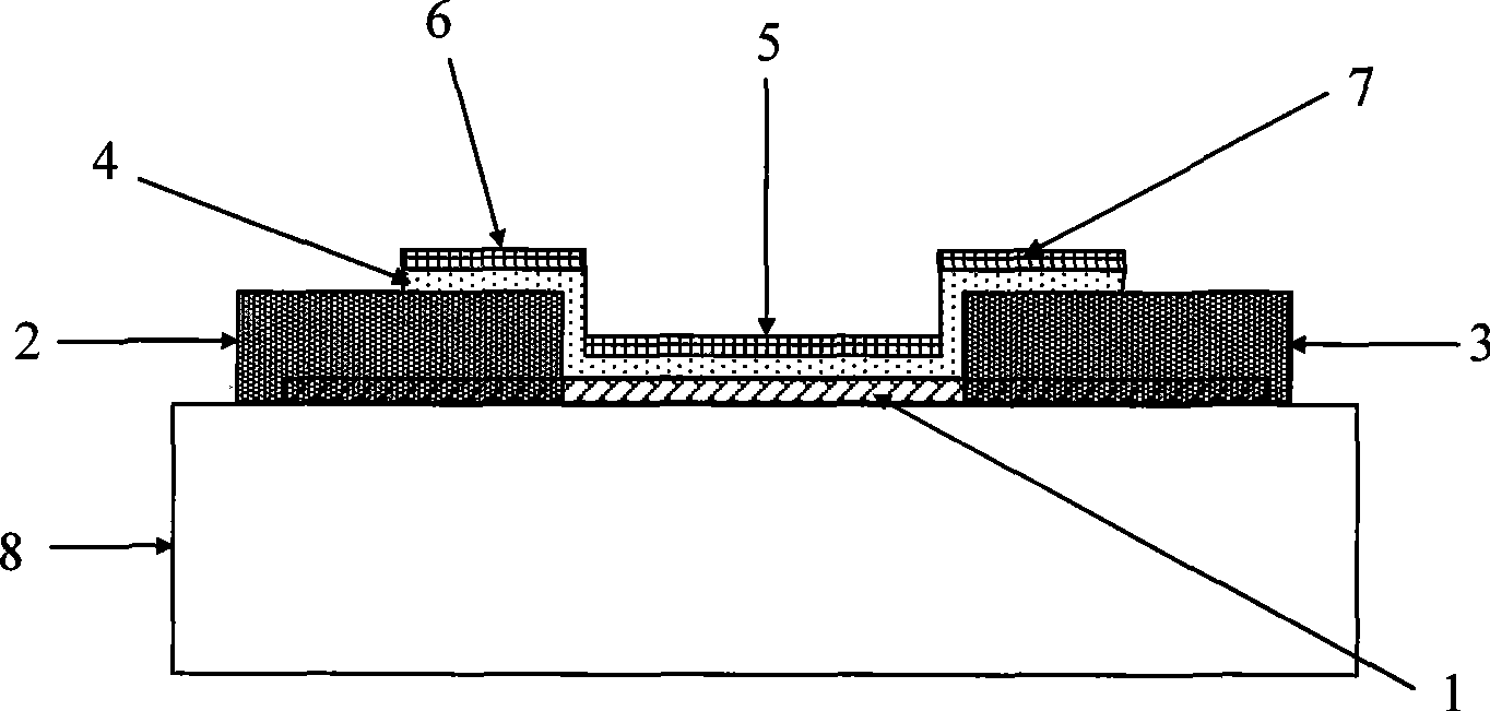
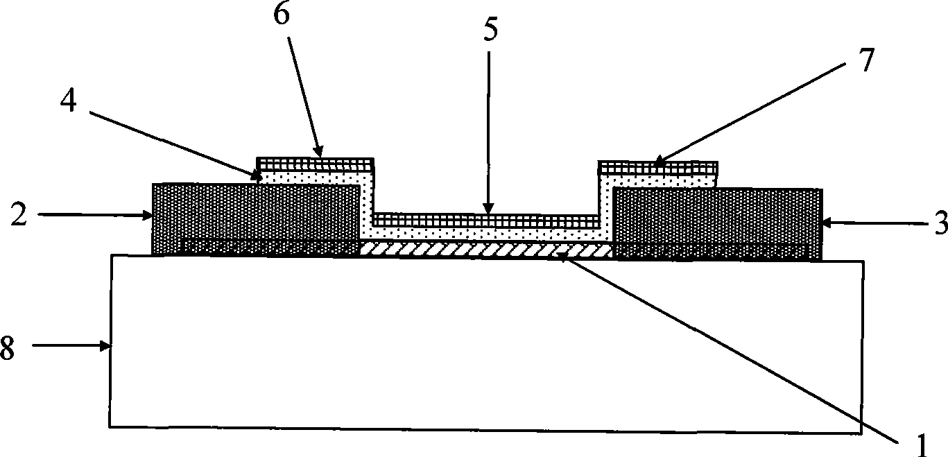
The invention discloses a self-aligned gate structure nano field-effect transistor and a process for preparation, wherein one-dimensional semiconductor nano material is used as a conductive channel whose two ends are respectively provided with a source electrode and a drain electrode, a gate dielectric layer is growth through using the atomic layer deposition way to be covered between the source electrode and the drain electrode and on the side walls of the opposite surfaces of the source electrode and the drain electrode, on parts of the source electrode and the drain electrode, a gate electrode layer is growth on the gate dielectric layer through the evaporation or sputtering ways, the sum of the thicknesses of the gate dielectric layer and the gate electrode layer is smaller than the thicknesses of the source electrode and the drain electrode, and the gate electrode on the conductive channel between the source electrode and the drain electrode is electrically isolated from the source electrode and the drain electrode through the gate dielectric side walls. The self-aligned structure of the invention has simple and stable fabrication process and high freedom, greatly increases the control capability of a gate for the conductive channel as the conductive channel is basically covered by the gate electrode, and has no limitations for the materials of the gate dielectric layer and the gate electrode layer, thereby freely adjusting the threshold voltage of components, and meeting the design requirements of a scale integrated circuit.
Description
Self-aligned gate structure nanometer field effect transistor and its preparation method field of invention The invention relates to a field effect transistor, in particular to a self-aligned field effect transistor constructed on the basis of one-dimensional semiconductor nanomaterials. Background technique Nanoelectronics based on semiconducting carbon nanotubes has great application prospects and is considered to be the most likely technology to replace the current silicon-based microelectronic integrated circuit process. Through nearly a decade of research, it has been realized that many nanoelectronic devices based on semiconductor carbon nanotubes, especially field effect transistors, have shown significantly better performance than silicon-based MOSFETs in terms of power consumption, speed and integration. Characteristics. In addition, since the polarity of the carbon nanotube field effect transistor depends on the properties of its source and drain electrode metal...
Claims
Login to View More Application Information
Patent Timeline
 Patent Type & AuthorityPatents(China)
IPC IPC(8): H01L29/78H01L29/41H01L29/423H01L21/336H01L21/28
CPCB82Y10/00H01L51/0048H01L29/0673H01L29/0665H01L51/0541Y10S977/938H10K85/221H10K10/464
Inventor彭练矛张志勇王胜梁学磊陈清
OwnerPEKING UNIV