Self-aligning gate construction nano field-effect transistor and preparation thereof

A field effect transistor and gate structure technology, applied in the field of self-aligned field effect transistors, can solve problems such as the inability to freely select metals

Active Publication Date: 2009-03-18
PEKING UNIV
View PDF0 Cites 18 Cited by
  • Summary
  • Abstract
  • Description
  • Claims
  • Application Information

AI Technical Summary

Problems solved by technology

However, the self-aligned structure of Dai makes it impossible to freely

Method used


Image

  • Self-aligning gate construction nano field-effect transistor and preparation thereof
  • Self-aligning gate construction nano field-effect transistor and preparation thereof
  • Self-aligning gate construction nano field-effect transistor and preparation thereof

Examples


Embodiment 1

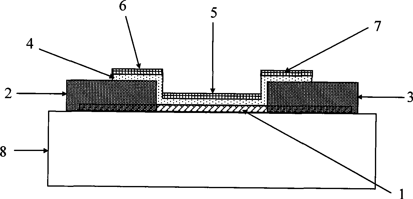
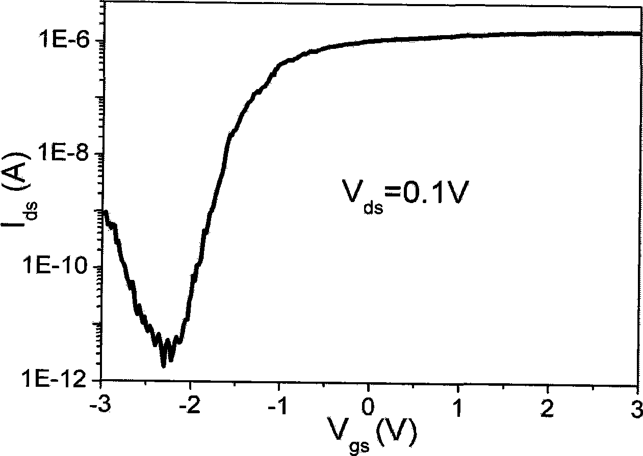
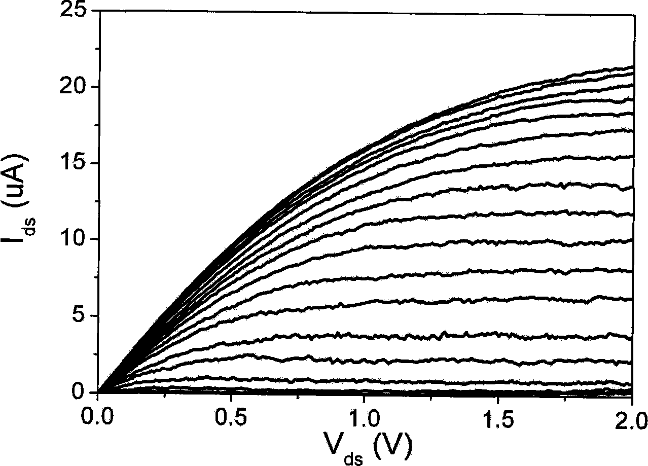
[0031] Such as figure 1 The shown metal scandium as the source and drain electrodes, HfO 2 The n-type self-aligned carbon nanotube field effect transistor is a gate dielectric and metal Ti is a gate electrode. The two Sc electrodes on the carbon nanotubes 1 distributed on the insulating substrate 8 are source electrodes 2 and drain electrodes 3 respectively, the gate dielectric layer is a hafnium oxide film 4 grown by ALD, and the gate electrode layer is a metal film grown by evaporation or sputtering , the portion 5 between the source and drain electrodes is disconnected from the portions 6 and 7 above the source and drain electrodes. Concrete preparation steps are as follows:

[0032] 1. Form the shape of the source and drain electrodes on the semiconductor carbon nanotubes by photolithography, evaporate a layer of Sc metal layer with a thickness of 80 nanometers as the source and drain electrode layers, and then put the sample into acetone to remove the unnecessary The m...


PUM

PropertyMeasurementUnit
Thicknessaaaaaaaaaa
Thicknessaaaaaaaaaa

Abstract

The invention discloses a self-aligned gate structure nano field-effect transistor and a process for preparation, wherein one-dimensional semiconductor nano material is used as a conductive channel whose two ends are respectively provided with a source electrode and a drain electrode, a gate dielectric layer is growth through using the atomic layer deposition way to be covered between the source electrode and the drain electrode and on the side walls of the opposite surfaces of the source electrode and the drain electrode, on parts of the source electrode and the drain electrode, a gate electrode layer is growth on the gate dielectric layer through the evaporation or sputtering ways, the sum of the thicknesses of the gate dielectric layer and the gate electrode layer is smaller than the thicknesses of the source electrode and the drain electrode, and the gate electrode on the conductive channel between the source electrode and the drain electrode is electrically isolated from the source electrode and the drain electrode through the gate dielectric side walls. The self-aligned structure of the invention has simple and stable fabrication process and high freedom, greatly increases the control capability of a gate for the conductive channel as the conductive channel is basically covered by the gate electrode, and has no limitations for the materials of the gate dielectric layer and the gate electrode layer, thereby freely adjusting the threshold voltage of components, and meeting the design requirements of a scale integrated circuit.

Description

field of invention [0001] The invention relates to a field effect transistor, in particular to a self-aligned field effect transistor constructed on the basis of one-dimensional semiconductor nanomaterials. Background technique [0002] Nanoelectronics based on semiconducting carbon nanotubes has great application prospects and is considered to be the most likely technology to replace the current silicon-based microelectronic integrated circuit process. Through nearly a decade of research, it has been realized that many nanoelectronic devices based on semiconductor carbon nanotubes, especially field effect transistors, have shown significantly better performance than silicon-based MOSFETs in terms of power consumption, speed and integration. Characteristics. In addition, since the polarity of the carbon nanotube field effect transistor depends on the properties of its source and drain electrode metals, it has been found that metal palladium can form an ohmic contact with th...

Claims


Application Information

Patent Timeline
IPC IPC(8): H01L29/78H01L29/41H01L29/423H01L21/336H01L21/28
CPCB82Y10/00H01L29/0665H01L51/0541H01L51/0048H01L29/0673Y10S977/938H10K85/221H10K10/464
Inventor 彭练矛张志勇王胜梁学磊陈清
Owner PEKING UNIV
Why Eureka
Try Eureka