Circuit board producing method

A manufacturing method and a circuit board technology, which are applied in multilayer circuit manufacturing, secondary processing of printed circuits, and coating of non-metallic protective layers, etc., can solve problems affecting the yield of fine lines, poor surface flatness, and dielectric layer depressions Abnormal and other issues

Inactive Publication Date: 2009-03-18
NAN YA PRINTED CIRCUIT BOARD CORPORATION
View PDF0 Cites 8 Cited by
  • Summary
  • Abstract
  • Description
  • Claims
  • Application Information

AI Technical Summary

Problems solved by technology

When the dielectric layer used in the traditional build-up method is cured, the solvent contained in it will volatilize with baking and heating. After curi...

Method used


Image

  • Circuit board producing method
  • Circuit board producing method
  • Circuit board producing method

Examples


Embodiment Construction

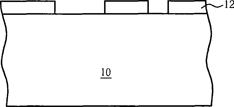
[0017] see Figure 1 to Figure 5 , which shows a schematic cross-sectional view of a preferred embodiment of the circuit board manufacturing method of the present invention. First, if figure 1 As shown, a substrate 10 is provided, and a first conductive pattern 12 is formed on the substrate 10 . The substrate 10 can be a circuit board with a conductive pattern or a circuit board without any conductive pattern. In addition, the first conductive pattern 12 is generally made of copper and formed through chemical deposition, lithography, and etching.

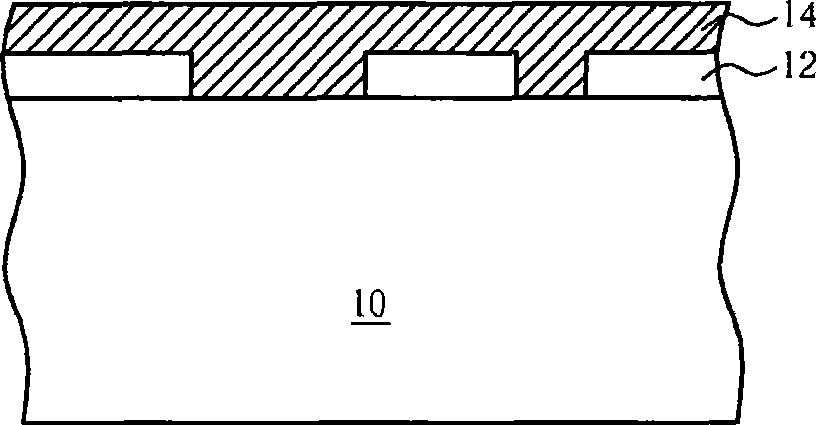
[0018] Next, if figure 2 As shown, a first dielectric layer 14 is formed on the substrate 10 to cover the surface of the substrate 10 and fill the gaps between the first wire patterns 12 as a build-up insulating layer. According to a preferred embodiment of the present invention, the method of forming the first dielectric layer 14 includes using a roller to coat the dielectric material on the surface of the substrate 10 and the ...


PUM


Abstract

The invention provides a manufacturing method for circuit board, which is characterized in that when manufacturing additional layered insulation layer of circuit board, a fist dielectric layer is firstly formed, and a second dielectric layer is formed subsequently after the curing process, that is the same layer of additional layered insulation layer is formed by two times of forming and curing steps. Therefore, problem of surface unevenness of the additional layered insulation layer is avoided, and yield of the fine line is improved. Moreover, because of using the same dielectric material by the first dielectric layer and the second dielectric layer, operation condition of the subsequent blind hole machining and coursing process of the additional layered insulation layer is easy to control.

Description

technical field [0001] The invention relates to a method for manufacturing a circuit board, in particular to a method for manufacturing a build-up insulation layer on a circuit board by a secondary lamination method to provide a better yield rate of fine lines. technical background [0002] Printed circuit boards usually use a build-up method to manufacture conductor lines. The build-up method can be laminated by dielectric film (Dielectric Film), and can also be laminated by adhesive backed copper foil (RCC) or prepreg (Prepreg). [0003] In general, the steps of the build-up method include: taking a substrate including a conductive via hole penetrating the substrate and a circuit pattern layer, filling the conductive via hole with a filler, and then laminating a dielectric layer on the surface of the substrate As a build-up insulating layer, wherein the dielectric layer covers the aforementioned circuit pattern layer and its gap, after curing, laser drilling is performed ...

Claims


Application Information

Patent Timeline
IPC IPC(8): H05K3/46H05K3/28
Inventor 廖恒纬叶昌幸林贤杰江国春
Owner NAN YA PRINTED CIRCUIT BOARD CORPORATION
Why Eureka
Try Eureka