

Full-integration ultraviolet micro-fluidic chip analyzer
A technology of microfluidic chips and analyzers, which is applied to the analysis of materials, material analysis through optical means, instruments, etc., can solve the problems of inability to realize multi-channel array detection, analysis throughput limitation, and short separation channel size, etc., to achieve Powerful functions, scalability, and user-friendly effects
- Summary
- Abstract
- Description
- Claims
- Application Information
AI Technical Summary
Problems solved by technology
Method used
Image

Examples
Embodiment
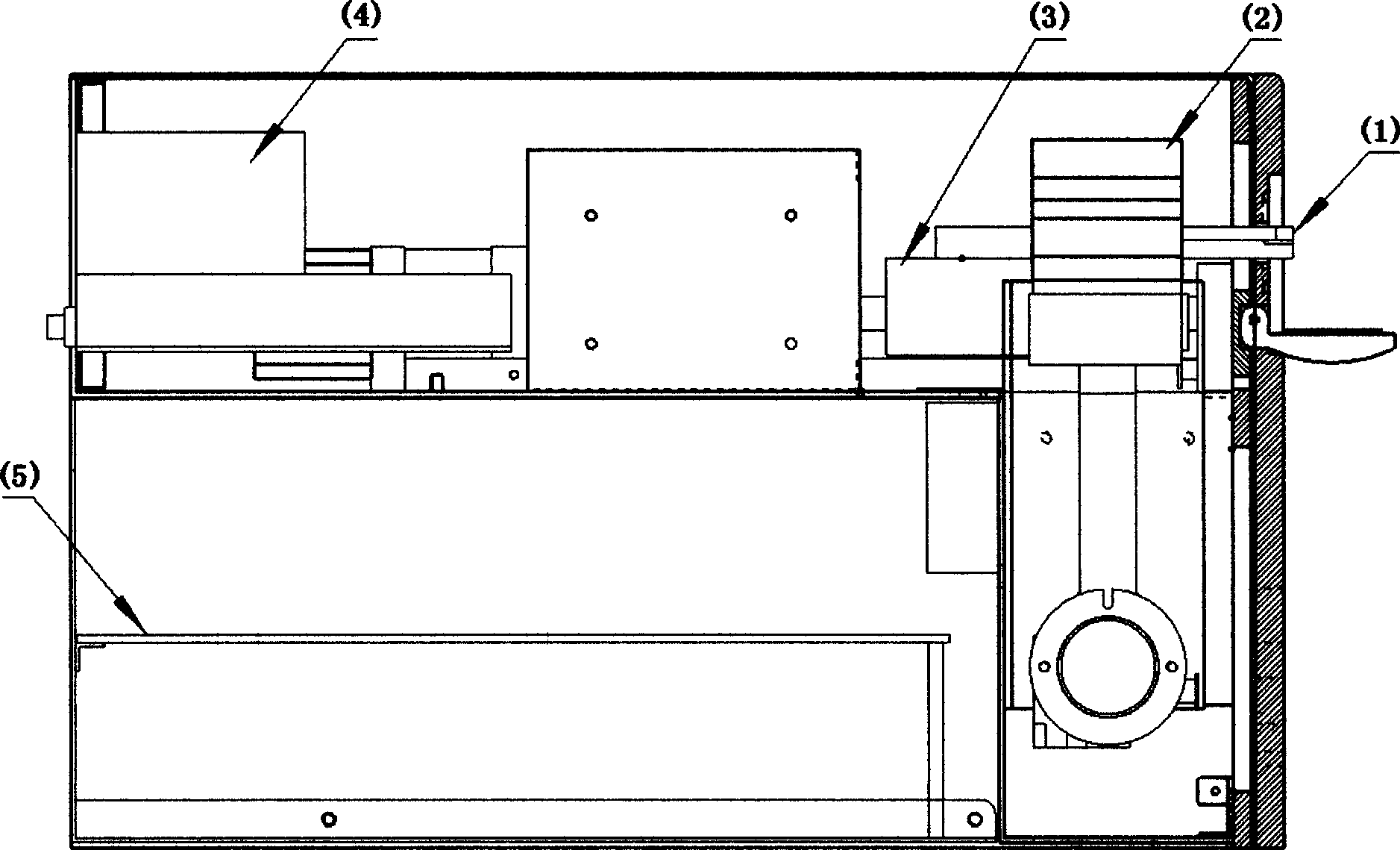
[0026] 1. Fully integrated UV microfluidic chip instrument structure
[0027] Such as figure 1 The hardware of the fully integrated ultraviolet microfluidic chip instrument shown includes a plug-in chip electrode plate (1) an ultraviolet detection optical system (2), a CD tray type chip mobile adjustment platform (3), a signal acquisition board (4), a high-voltage power supply and control panel (5);
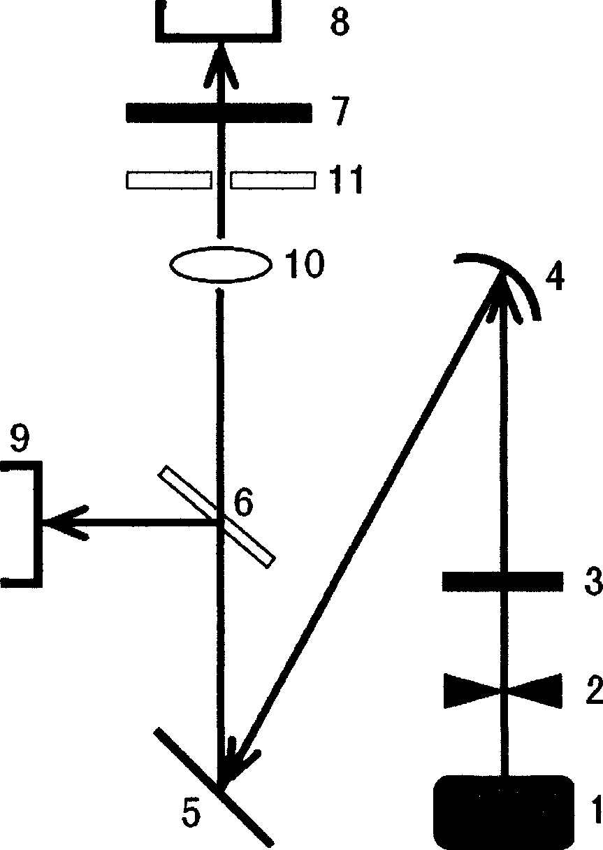
[0028] The ultraviolet detection optical path system (2) includes a deuterium lamp 1, a slit 2, an optical filter 3, a concave mirror 4, a plane grating 5, a beam splitter 6, a chip channel 7, a sample photodiode 8, a reference photodiode 9, Cylindrical mirror 10, rectangular light hole 11;
[0029] The main power supply, chip platform movement control and detection channel optical alignment buttons are located in front of the casing panel, the ultraviolet detection wavelength setting panel, CD tray type chip movement adjustment platform window are located in front of the casin...
PUM
 Abstract
Description
Claims
Application Information