Wafer, test system thereof, test method thereof, and test fixture thereof
A technology of wafer testing and fixtures, which is applied in semiconductor/solid-state device testing/measurement, electronic circuit testing, single semiconductor device testing, etc., to achieve the effect of reducing test time
- Summary
- Abstract
- Description
- Claims
- Application Information
AI Technical Summary
Problems solved by technology
Method used
Image

Examples
Embodiment Construction
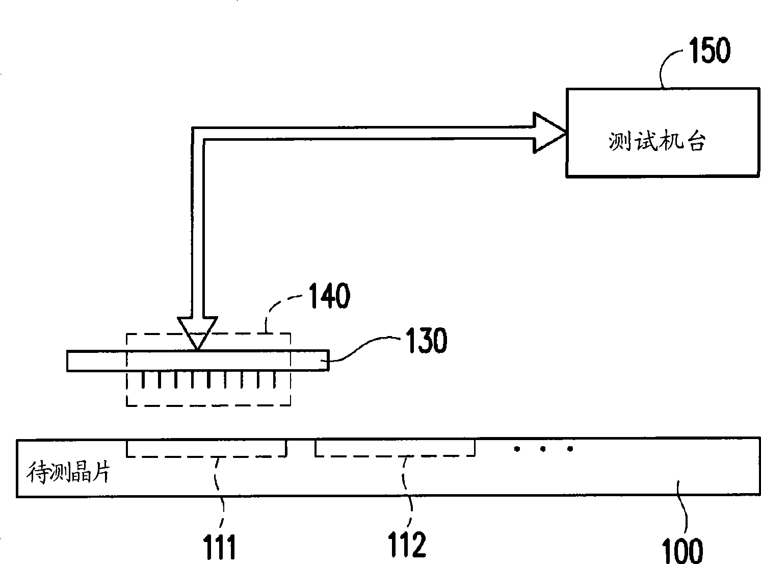
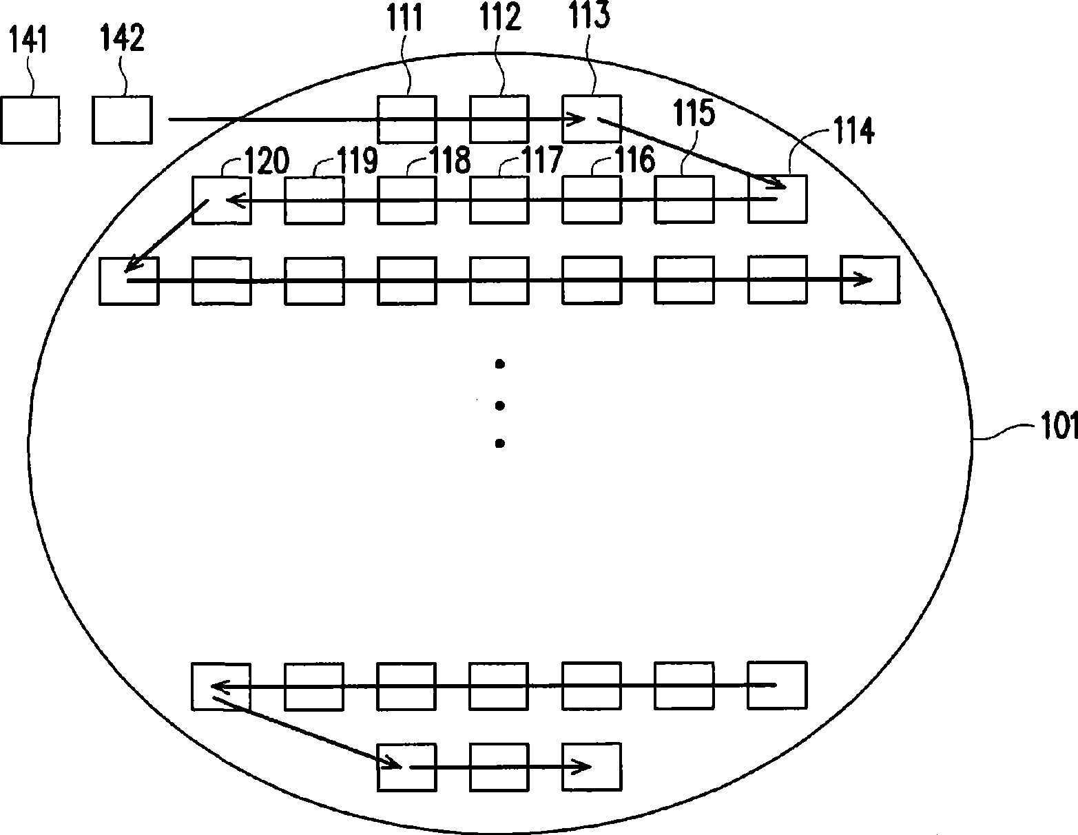
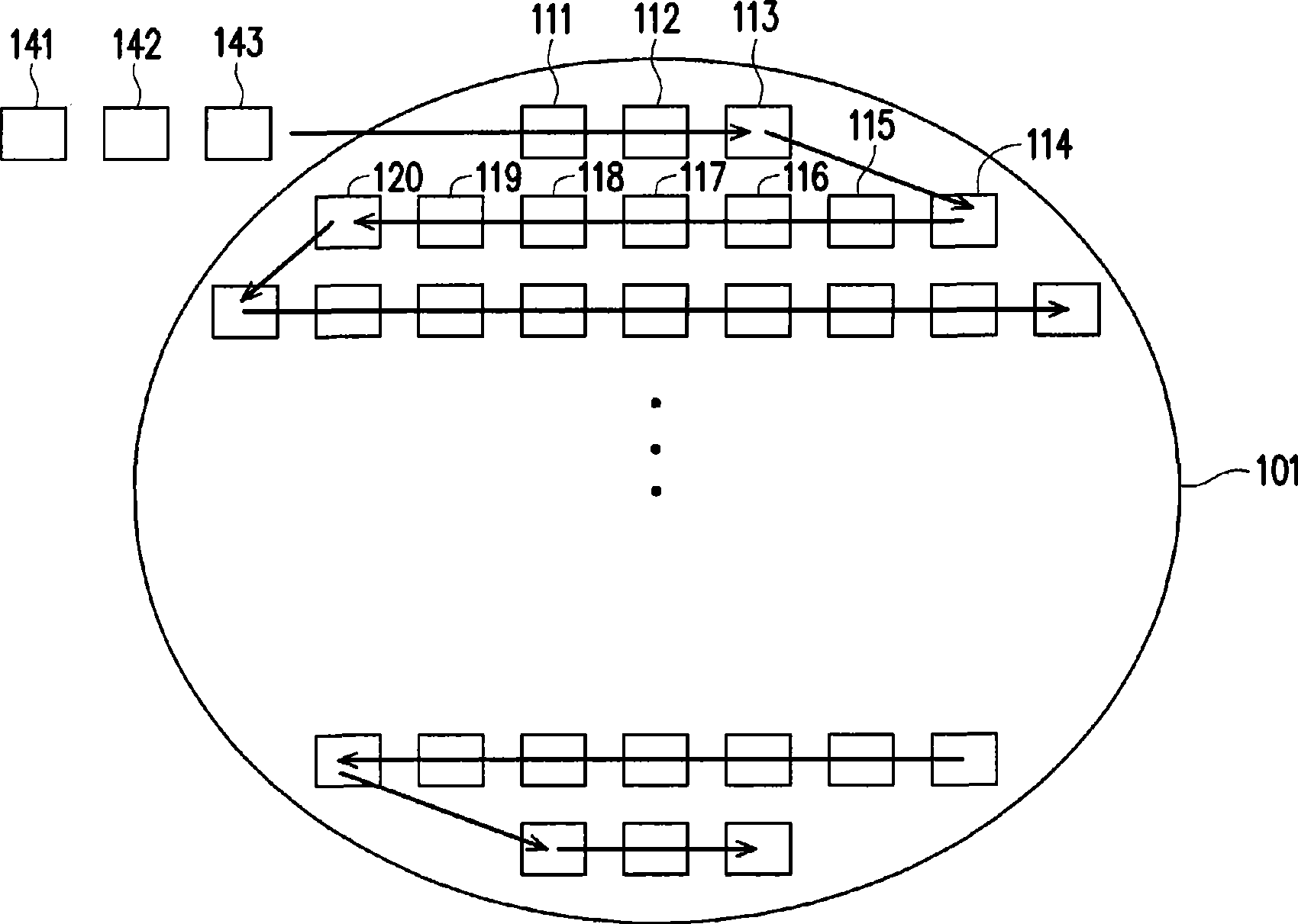
[0044] Generally speaking, the CP test on the chip can be divided into two stages: HVS test and functional test. Taking the chip of the source driver as an example, the functional test not only needs to provide a test signal to the input terminal of the chip, but also needs to detect whether the signal at the output terminal of the chip is normal, so about 600-700 probes are needed to perform the functional test. .
[0045] It is worth noting that the purpose of the HVS test is to give the chip a higher than the rated operating voltage, so that the defective chip will deteriorate in a very short time, so that the defective chip can be detected more easily during the functional test. chip. Therefore, in practical applications, when performing HVS testing, it is only necessary to provide a test signal to the input terminal of the chip so that the chip is in a high-voltage operation state. "Is the chip normal?", then it can be tested together when the chip is functionally teste...
PUM
 Abstract
Description
Claims
Application Information
 - Generate Ideas
- Intellectual Property
- Life Sciences
- Materials
- Tech Scout
- Unparalleled Data Quality
- Higher Quality Content
- 60% Fewer Hallucinations
Browse by: Latest US Patents, China's latest patents, Technical Efficacy Thesaurus, Application Domain, Technology Topic, Popular Technical Reports.
© 2025 PatSnap. All rights reserved.Legal|Privacy policy|Modern Slavery Act Transparency Statement|Sitemap|About US| Contact US: help@patsnap.com