


Quick Research
Generate reliable direction feasibility study reports for your R&D in just a few steps.

Technical Q&A
Discover and master advanced knowledge NOW. Basics, ideas, possibilities, all at once.

Find Solutions
As an expert in R&D theories, this can generate solutions to your technical problems instantly.

Evaluate Feasibility
Analyze your overall solution with one click, know your potential R&D risks in advance.

Monitor Landscape
Get weekly tech updates, stay abreast of the latest tech innovations and key insights.
DVI-I and VGA interface circuit
A technology of DVI-I and VGA interface, applied in the design of DVI and VGA output circuits of embedded systems, in the field of DVI-I and VGA interface circuits, can solve problems such as no public reports, and achieve the effect of simple structure
- Summary
- Abstract
- Description
- Claims
- Application Information
AI Technical Summary
Problems solved by technology
Method used
Image

Examples
Embodiment 1
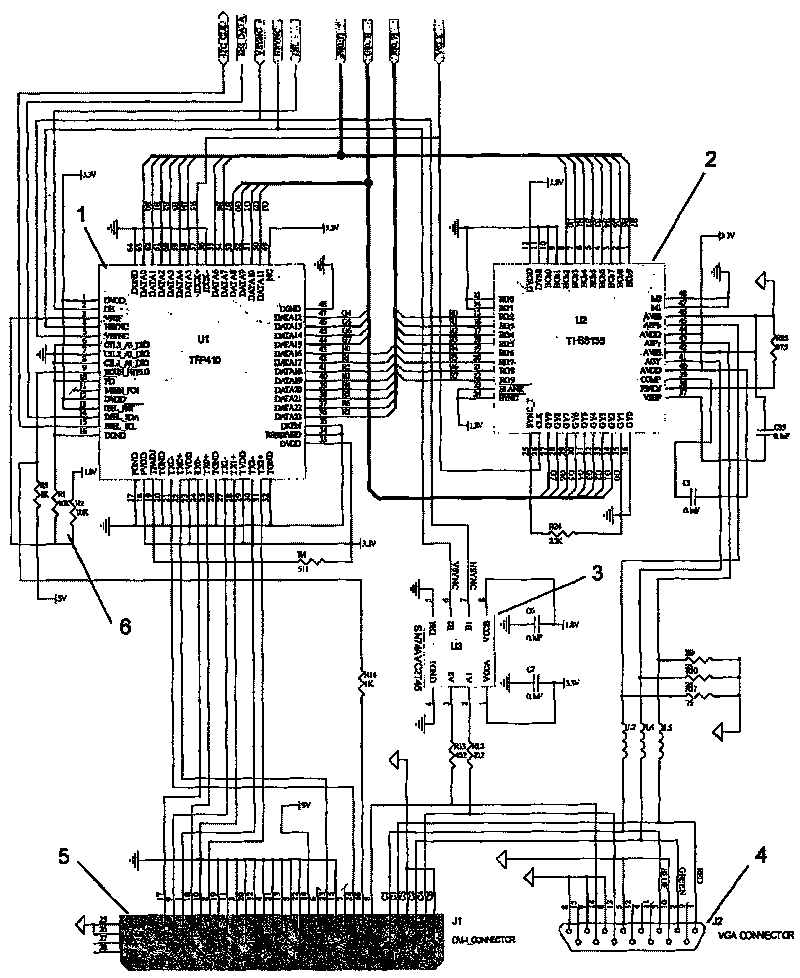
[0017] It is suitable for systems where the output signal of the media processor is 1.8V level. Such as figure 1 Shown: The circuit consists of TFP410DVI transmitter chip 1, THS8135 three-way video DAC conversion chip 2, 74AVC2T451.8V to 3.3V level conversion chip 3, VGA output socket 4, DVI-I output socket 5 and reference voltage divider resistor 6 composition. The 1.8V level signal R, G, B data lines and VCLK video clock lines from the media processor are respectively connected to the data input pins and clock input tubes of TFP410DVI transmitter chip 1 and THS8135 three-way video DAC conversion chip 2 pin; the video data enable signal DE is connected to the DE input pin of TFP410; the line and field synchronization signals HSYNC and VSYNC are connected to the line and field synchronization signal pins of TFP410 at the same time, and the 1.8V level is converted to meet the requirements of the VGA interface through 74AVC2T45 After the 3.3V level, it is connected to the VGA ...
Embodiment 2
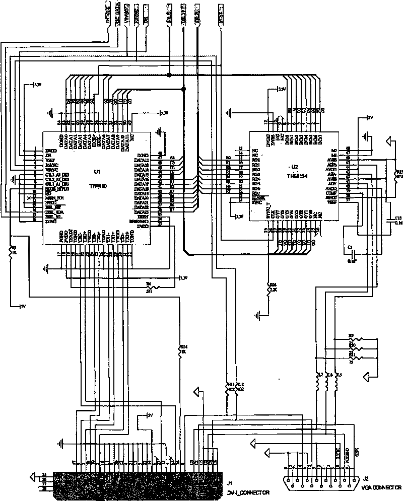
[0019] It is suitable for systems where the output signal of the media processor is 3.3V level. Such as figure 2 As shown: the circuit is composed of TFP410DVI transmitter chip 1, THS8134 three-way video DAC conversion chip 2, VGA output socket 4 and DVI-I output socket 5. Since the digital signal to be processed is a 3.3V level signal, at this time, the three-way video DAC conversion chip adopts THS8134 to directly process the 3.3V level signal; the line and field synchronization signals HSYNC and VSYNC do not need to be level converted, and are directly connected to the VGA socket and DVI-I socket; the VREF pin of TFP410 does not need to be divided by a voltage divider resistor, and is directly connected to the 3.3V voltage.
[0020] Use shows: a kind of DVI-I of the present invention and VGA interface circuit, structure is simple, support bandwidth is high, support high-definition resolution, support DVI and VGA dual-port display output on the same screen, and debugging i...
PUM
 Abstract
Description
Claims
Application Information
 - R&D Engineer
- R&D Manager
- IP Professional
- Industry Leading Data Capabilities
- Powerful AI technology
- Patent DNA Extraction
Browse by: Latest US Patents, China's latest patents, Technical Efficacy Thesaurus, Application Domain, Technology Topic, Popular Technical Reports.
© 2024 PatSnap. All rights reserved.Legal|Privacy policy|Modern Slavery Act Transparency Statement|Sitemap|About US| Contact US: help@patsnap.com