Apparatus and method for preventing snap back in integrated circuits

A circuit, bias circuit technology, applied in the direction of electrical components, generation of electrical pulses, reliability improvement and modification, etc., can solve problems such as backup current flow, data corruption, etc.

Inactive Publication Date: 2009-04-15
ATMEL CORP
View PDF0 Cites 0 Cited by
  • Summary
  • Abstract
  • Description
  • Claims
  • Application Information

AI Technical Summary

Problems solved by technology

The high-voltage N-channel driver is draining, causing standby current to flow during standby
This also causes the latch circuit to flip state during high voltage operation, resulting in data corruption

Method used


Image

  • Apparatus and method for preventing snap back in integrated circuits
  • Apparatus and method for preventing snap back in integrated circuits

Examples


Embodiment Construction

[0008] Those skilled in the art will realize that the following description of the invention is illustrative only and not limiting in any way. Other embodiments of the invention will be readily apparent to those skilled in the art.

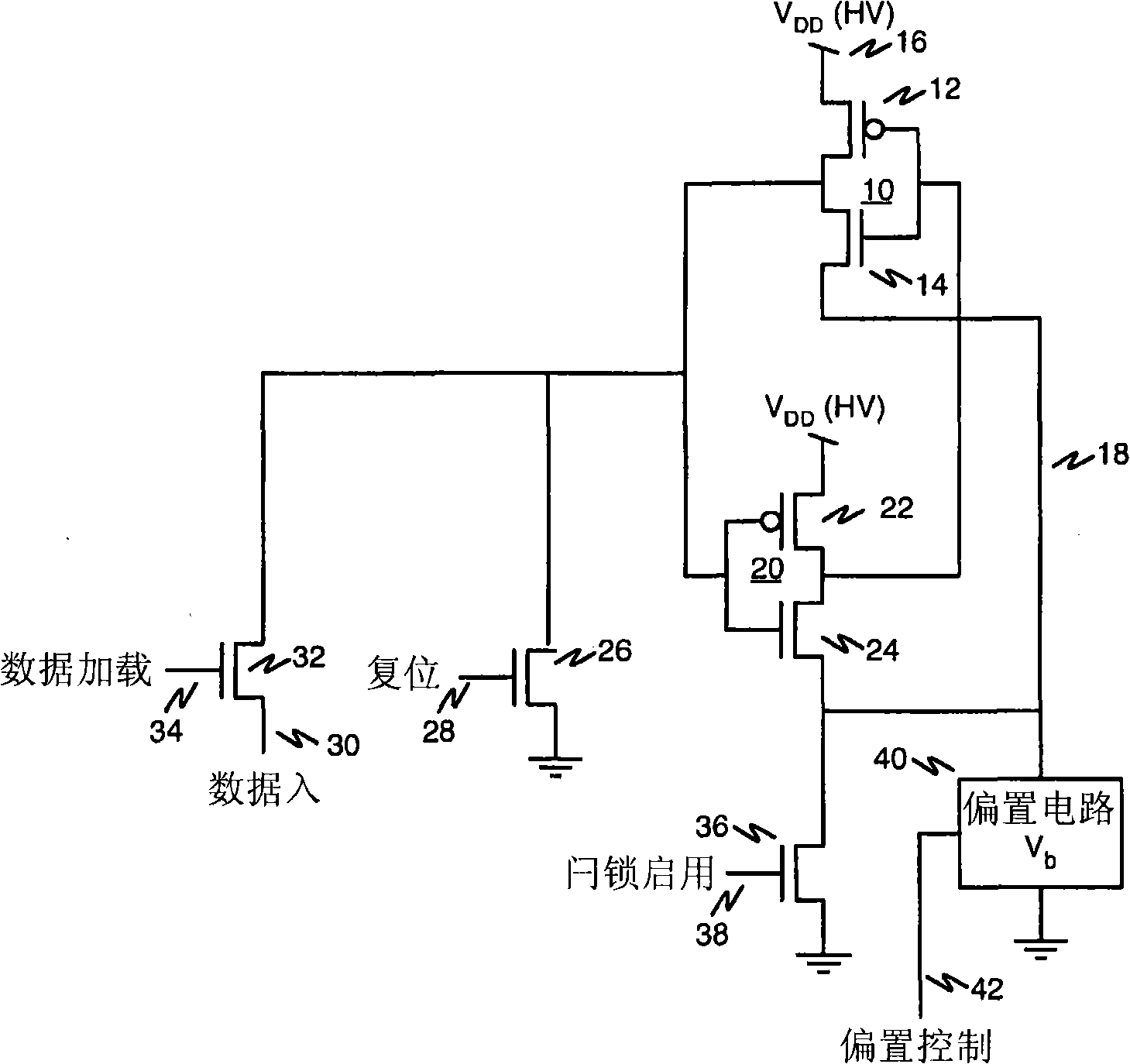
[0009] According to an illustrative example of a device according to the invention, such as figure 1 As shown in , the first inverter 10 includes a P-channel MOS transistor 12 connected in series with an N-channel MOS transistor 14 at the high voltage source V HV (shown at reference numeral 16 ) (eg 16V) and source node 18 . The gates of transistors 12 and 14 are coupled together. The second inverter 20 includes a P-channel MOS transistor 22 connected in series with an N-channel MOS transistor 24 between the high voltage source 16 and the source node 18 . The gates of transistors 22 and 24 are coupled together. Transistors 12, 14, 22 and 24 are high voltage transistors, ie transistors designed to have a breakdown voltage higher than the VDD vo...


PUM


Abstract

A method for preventing snap-back in a circuit including at least one MOS transistor having a parasitic bipolar transistor associated with it includes coupling a circuit node including at least one source / drain node of the at least one MOS transistor to a bias-voltage circuit and enabling the bias-voltage circuit to supply a potential to the at least one source / drain node of the at least on MOS transistor, the potential having a magnitude selected to prevent the parasitic bipolar transistor from turning on.

Description

technical field [0001] The present invention relates to integrated circuit technology. Background technique [0002] Snapback has become a problem in integrated circuits when voltages exceeding the junction breakdown of transistor devices are present in the integrated circuit. This problem is currently addressed by providing guard ring structures known in the art. The guard ring structure only minimizes snapback but does not eliminate snapback. [0003] In circuits such as non-volatile memories, high voltage P-channel and N-channel MOS transistor devices are used to form latch circuits to store written data. The high-voltage N-channel driver is leaky, causing standby current to flow during standby. This also causes the latch circuit to flip state during high voltage operation, leading to data corruption. [0004] Toggle phases and data corruption in high voltage latch circuits are caused by snapback of high voltage N-channel or P-channel devices during high voltage opera...

Claims


Application Information

Patent Timeline
Patent Type & Authority Applications(China)
IPC IPC(8): H03K19/003
CPCH03K3/013H03K3/356182
Inventor 菲利普·额曾赛凯克里斯·李王立琦孙晋书
Owner ATMEL CORP
Why Eureka
Try Eureka