Probe column, wafer testing seat and wafer testing system

A wafer test and probe technology, applied in the field of probe towers, can solve problems such as easy breakage of needles

Active Publication Date: 2009-05-06
KING YUAN ELECTRONICS
View PDF5 Cites 11 Cited by
  • Summary
  • Abstract
  • Description
  • Claims
  • Application Information

AI Technical Summary

Problems solved by technology

[0008] In order to solve the above problems and achieve the purpose of eliminating noise and leakage current, the present invention discloses the appropriate test probe outer diameter and the aperture size of the probe tower body for placing the test probe through calculation, so as to solve the problem of the calibration of the test probe. When the machine is machined, the needle part is easy to break
Then...

Method used


Image

  • Probe column, wafer testing seat and wafer testing system
  • Probe column, wafer testing seat and wafer testing system
  • Probe column, wafer testing seat and wafer testing system

Examples


no. 5 example

[0053] Please refer to Figure 8 , which is a fifth embodiment provided according to the present invention, is a wafer testing method. This test method consists of the following steps:

[0054] (1) Provide a wafer 5 to be tested (step 51).

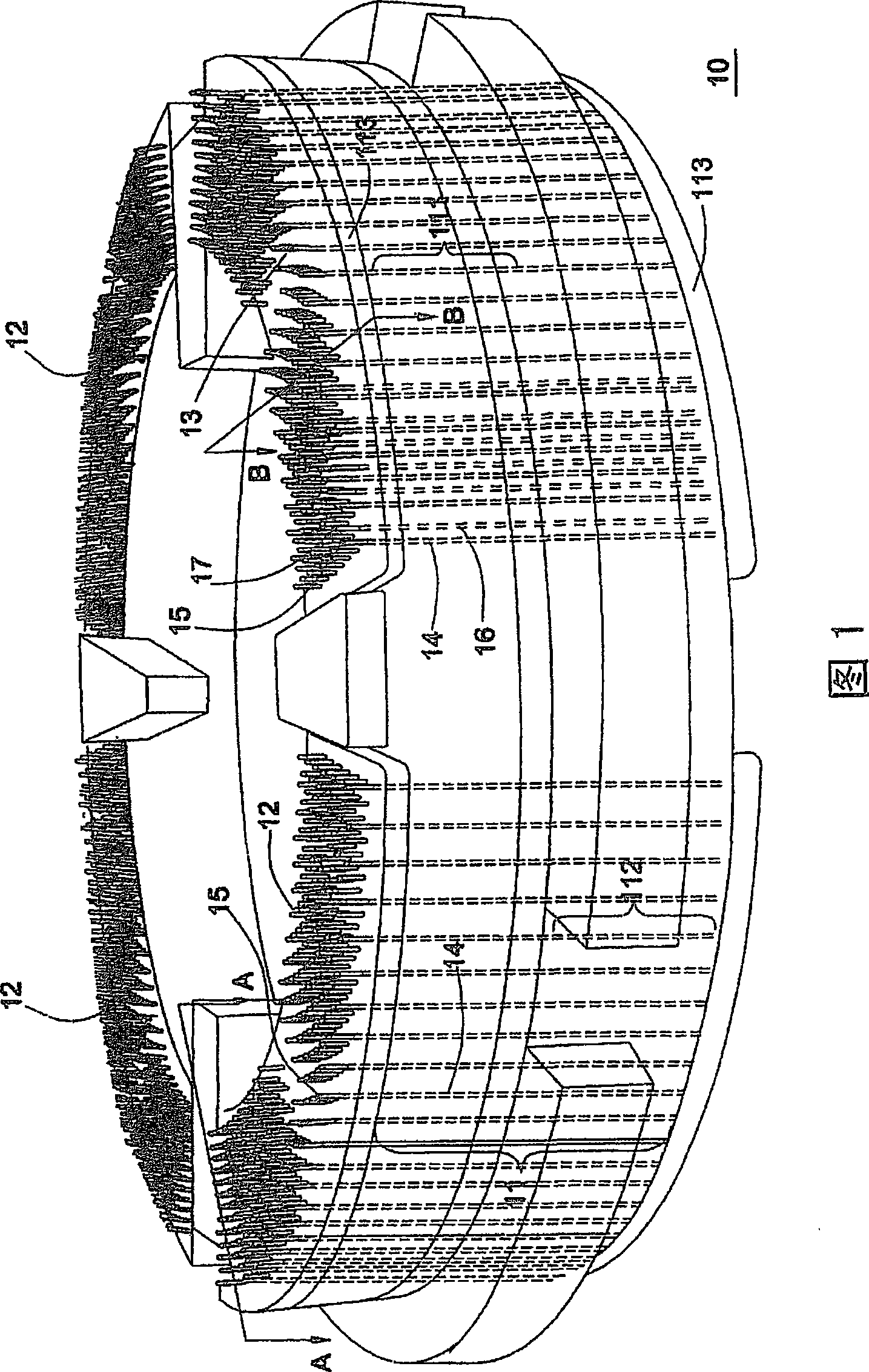
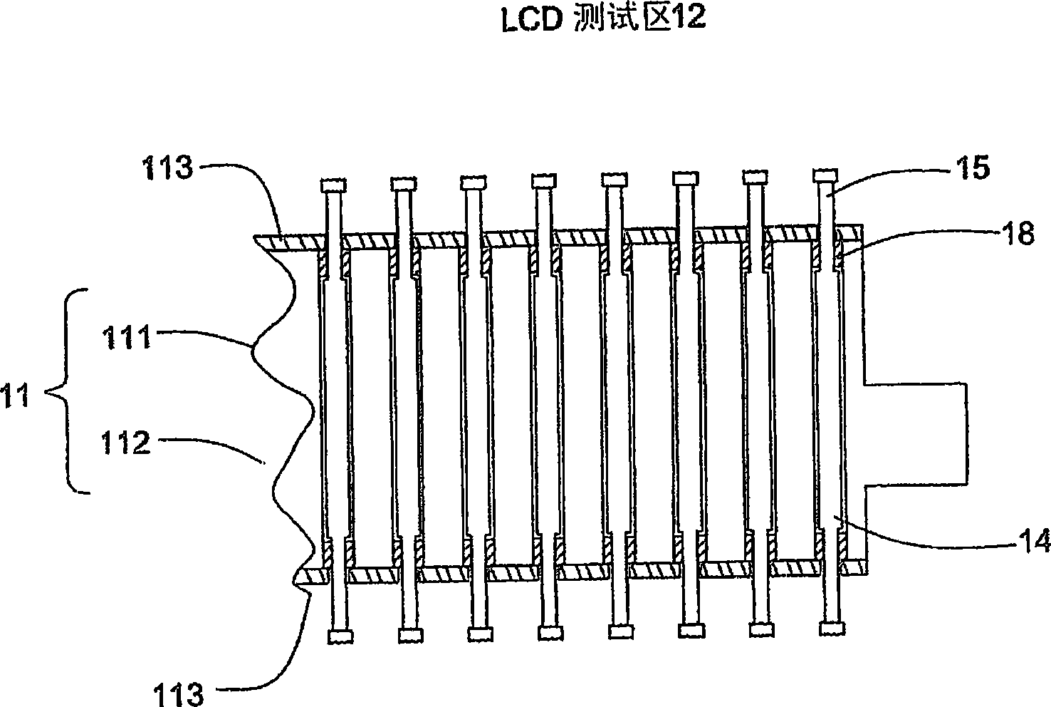
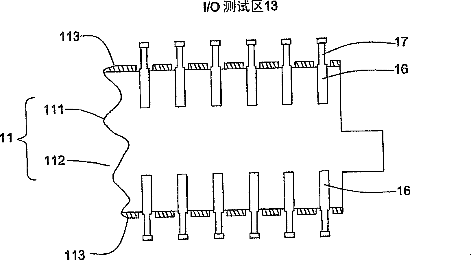
[0055] (2) Provide a wafer test seat 51 (step 52 ), which at least has a moving platform 52 , a probe tower 50 and a needle test card 53 . The motion platform 52 is used to carry a wafer 54 to be tested and provide its movement in the three axes of X-Y-Z. The needle test card 53 provides contact with the wafer 54 to be tested, and connects the electrical signal to be tested on the wafer 54 to be tested, and then performs relevant signal analysis and processing after receiving the signal through the probe tower 50 . The technical features and related structures of the probe tower 50 are as described for the probe tower 10 of the first embodiment.

[0056] (3) Provide a test head 55 (step 53 ) for correspondingly connecting to the probe ...


PUM


Abstract

The invention discloses a probe tower used for testing wafers, which comprises a circular body, a plurality of probe holes, a plurality of testing probes, a plurality of grounding holes, a plurality of grounding pins and a plurality of spacer rings, wherein the circular body is provided with an LCD testing area, an I/O testing area and an upper and a lower seats of the body; the probe holes are formed on the LCD and the I/O testing areas and vertically penetrate through the upper and the lower seats of the body; the testing probes are arranged in the probe holes so as to transfer testing signals passing through the circular body; the grounding holes are formed on the I/O testing area; the grounding pins are closely fitted in the grounding holes of the upper or the lower seat of the body and electrically conduct the circular body so as to ground the noise and the drain current of the adjacent testing probes; the spacer rings are made from insulation materials and are arranged on the ends of the probe holes so as to fix the testing probes on the circular body; and besides, the spacer rings electrically insulate the testing probes from the circular body.

Description

technical field [0001] The present invention relates to a pogo tower, in particular to a pogo tower with effects of reducing noise and leakage current. Background technique [0002] At present, the test probes on the probe tower are respectively arranged in the I / O area and the LCD area of ​​the probe tower. The test probes used in the I / O area are thinner, and the test probes used in the LCD area are thicker. At present, the test probes in the I / O area and LCD area of ​​the probe tower are fixed. The part of the test probe casing is soldered to the PCB board first, and then the test probe needle is put into the test probe. In the bushing, and use the wires on the PCB board to connect the I / O area and the ground of the LCD area to each other, so as to eliminate noise and leakage current. U.S. Patent No. 6,114,869, U.S. Patent No. 6,166,553, and U.S. Patent No. 63,040 of known technologies [0003] No. 92, US Pat. No. 6,741,072, and US Pat. No. 6,876,215 all disclose basic ...

Claims


Application Information

Patent Timeline
IPC IPC(8): G01R1/073G01R31/00G01R31/26G01R31/28
Inventor 林源记黎孟达
Owner KING YUAN ELECTRONICS
Why Eureka
Try Eureka