Byproduct collecting apparatus of semiconductor apparatus

A technology for reacting by-products and shells, which is applied in the field of by-product collection devices, can solve the problems of TAT extension, reduced working rate, narrow collection area (narrow space), etc., and achieves the effects of reducing productivity, prolonging work cycle and improving collection efficiency.

Active Publication Date: 2009-05-13
MILAEBO
View PDF0 Cites 12 Cited by
  • Summary
  • Abstract
  • Description
  • Claims
  • Application Information

AI Technical Summary

Problems solved by technology

Therefore, not only the working rate of the equipment is reduced, but also the TAT is prolonged due to the long standby time of the processing chamber
[0008]Secondly, since the collection area (space) of the capture duct for powder accumulation is very narrow, the powder accumulated in the capture duct must be removed frequently, which is very difficult. inconvenient
In particular, the cleaning cycle of the catch pipe is very short since the powder is only concentrated and accumulated at the inlet of the catch pipe

Method used


Image

  • Byproduct collecting apparatus of semiconductor apparatus
  • Byproduct collecting apparatus of semiconductor apparatus
  • Byproduct collecting apparatus of semiconductor apparatus

Examples


Embodiment Construction

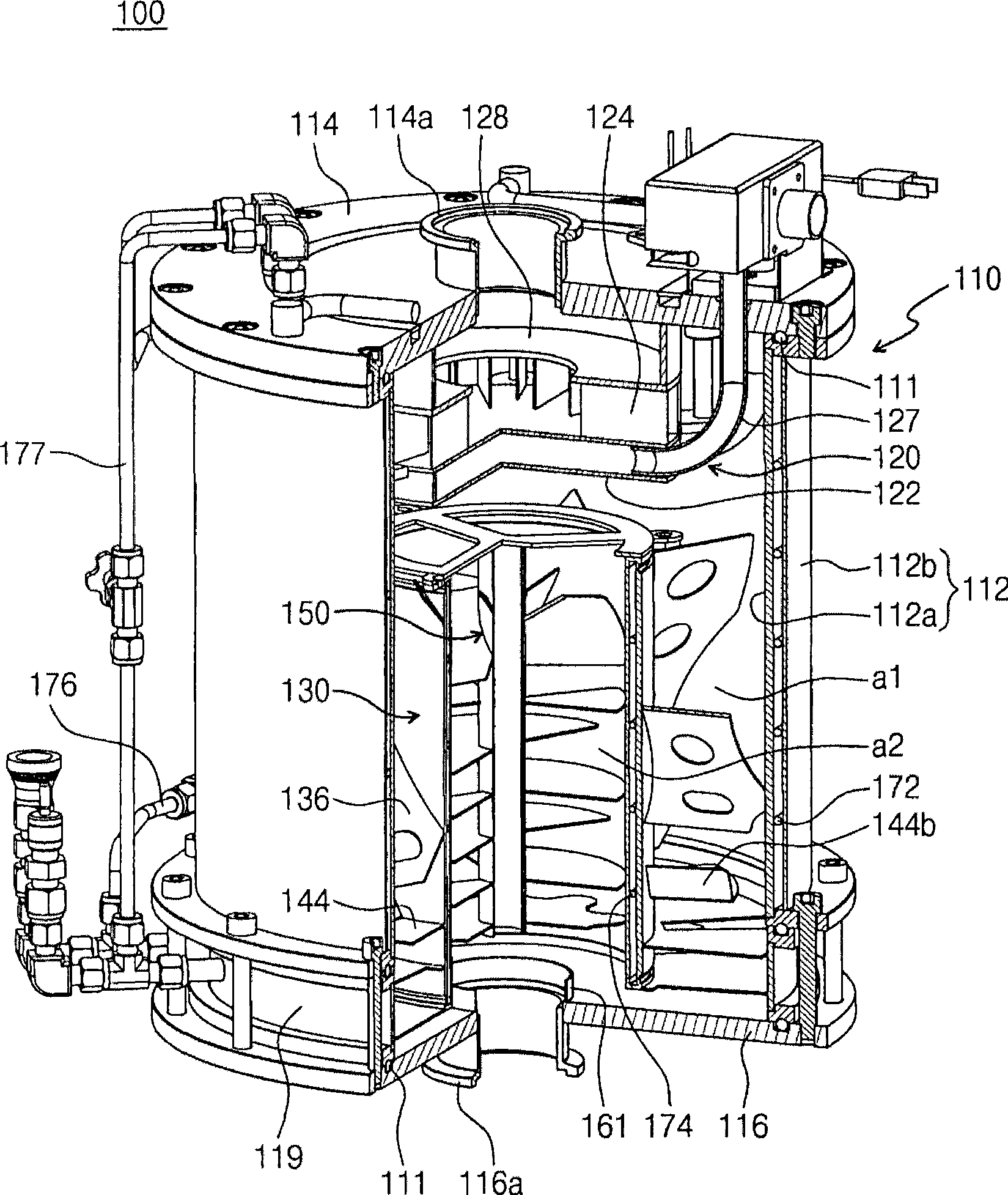
[0053] The structure of the collecting device of the invention allows the exhaust gases to pass through a simple and wide channel at the front and through a complex and narrow channel at the rear, so that the powder can not only accumulate evenly on the front, but also build up on the rear. In addition, the structure of the collecting device of the present invention can double cool the temperature of the exhaust gas on the outside and inside of the casing, thereby reducing the temperature of the exhaust gas more quickly.

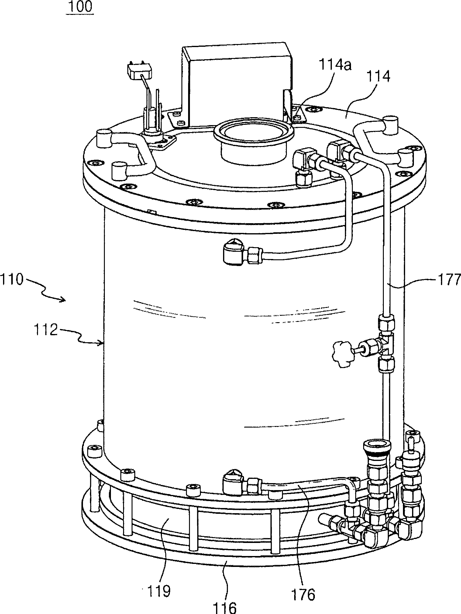
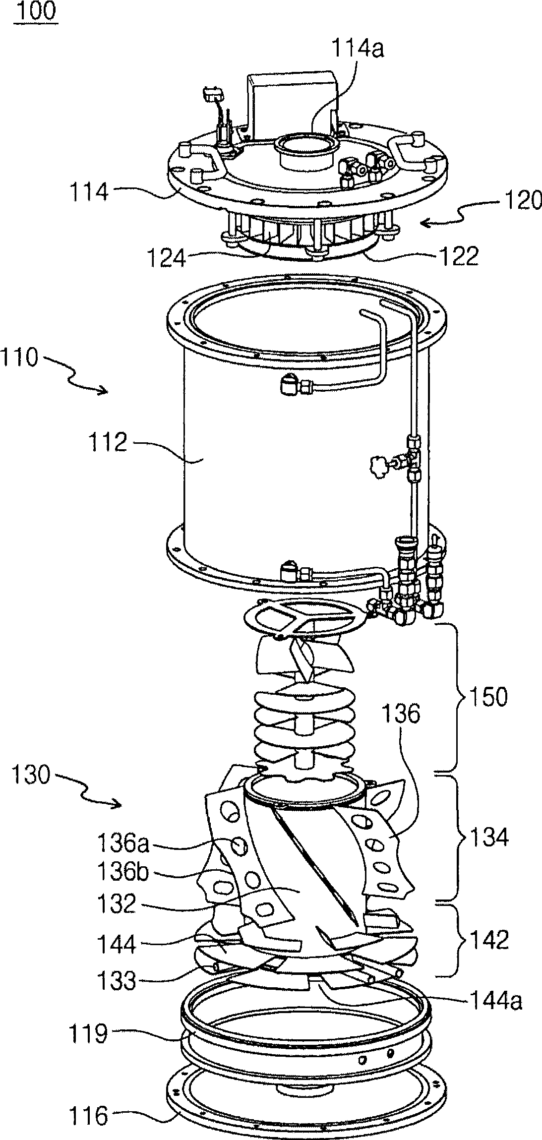
[0054] figure 1 is a view illustrating the appearance of a by-product collecting device of an embodiment of the present invention, figure 2 is a partial cross-sectional view of the by-product collection device, image 3 is an exploded perspective view of the by-product collection device, Figure 4 is a side view illustrating the by-product collection device, and Figure 5 is along Figure 4 A cross-sectional view of line A-A in .

[0055] The by-prod...


PUM

PropertyMeasurementUnit
angleaaaaaaaaaa

Abstract

Provided is a byproduct collecting apparatus for efficiently collecting reaction-byproducts contained in an exhaust gas exhausted from a process chamber during a semiconductor manufacturing process. The apparatus includes a housing and a trap module. The housing has a gas inlet port and a gas outlet port. The trap module is installed inside the housing and has first plates curved or inclined to guide an exhaust gas flow in a curved fashion.

Description

technical field [0001] The present invention relates to a by-product collection device for efficiently collecting reaction by-products contained in exhaust gas discharged from a process chamber during a semiconductor manufacturing process. Background technique [0002] Generally, the semiconductor manufacturing process is divided into a pre-processing process (manufacturing process) and a post-processing process (assembly process). The preprocessing process refers to a process of manufacturing a semiconductor chip by forming a predetermined pattern by repeatedly performing a process of depositing a thin film on a wafer in various processing chambers and selectively etching the deposited thin film. The post-processing process refers to the process of assembling a complete product by separating the chips manufactured in the pre-processing process into independent chips and combining these independent chips with a lead frame. In this regard, the process of depositing a thin fi...

Claims


Application Information

Patent Timeline
Patent Type & Authority Applications(China)
IPC IPC(8): H01L21/00H01L21/02
CPCB01D8/00B01D45/08B01D51/02B01D2258/0216F16L55/07H01L21/02
Inventor 赵宰孝洪正义金泰佑黄仁文
Owner MILAEBO
Why Eureka
Try Eureka