Method for monitoring etching process using optical emission spectrum characteristics

An etching process and optical emission technology, which is applied in semiconductor/solid-state device testing/measurement, electrical components, semiconductor/solid-state device manufacturing, etc., can solve problems such as difficult monitoring and achieve effective monitoring

Active Publication Date: 2009-05-20
SHANGHAI HUAHONG GRACE SEMICON MFG CORP
View PDF0 Cites 5 Cited by
  • Summary
  • Abstract
  • Description
  • Claims
  • Application Information

AI Technical Summary

Problems solved by technology

However, this is only a post-measurement method, that is, a method of measuring after a period of time after etching; and generally only one wafer is measured in a batch of prepared wafers, so it is difficult to realize real-time and effective monitoring

Method used


Image

  • Method for monitoring etching process using optical emission spectrum characteristics
  • Method for monitoring etching process using optical emission spectrum characteristics
  • Method for monitoring etching process using optical emission spectrum characteristics

Examples


Embodiment Construction

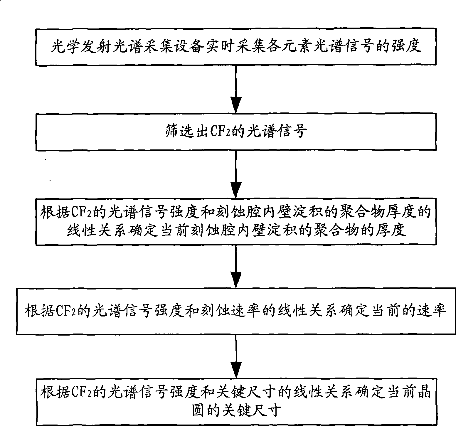
[0017] The method for monitoring the etching process by using optical emission spectrum characteristics of the present invention will be further described in detail below.

[0018] See figure 1 , the method of the present invention comprises the following steps:

[0019] First, during the etching process, the optical emission spectrum acquisition equipment collects the intensity of the spectral signal of each element in real time.

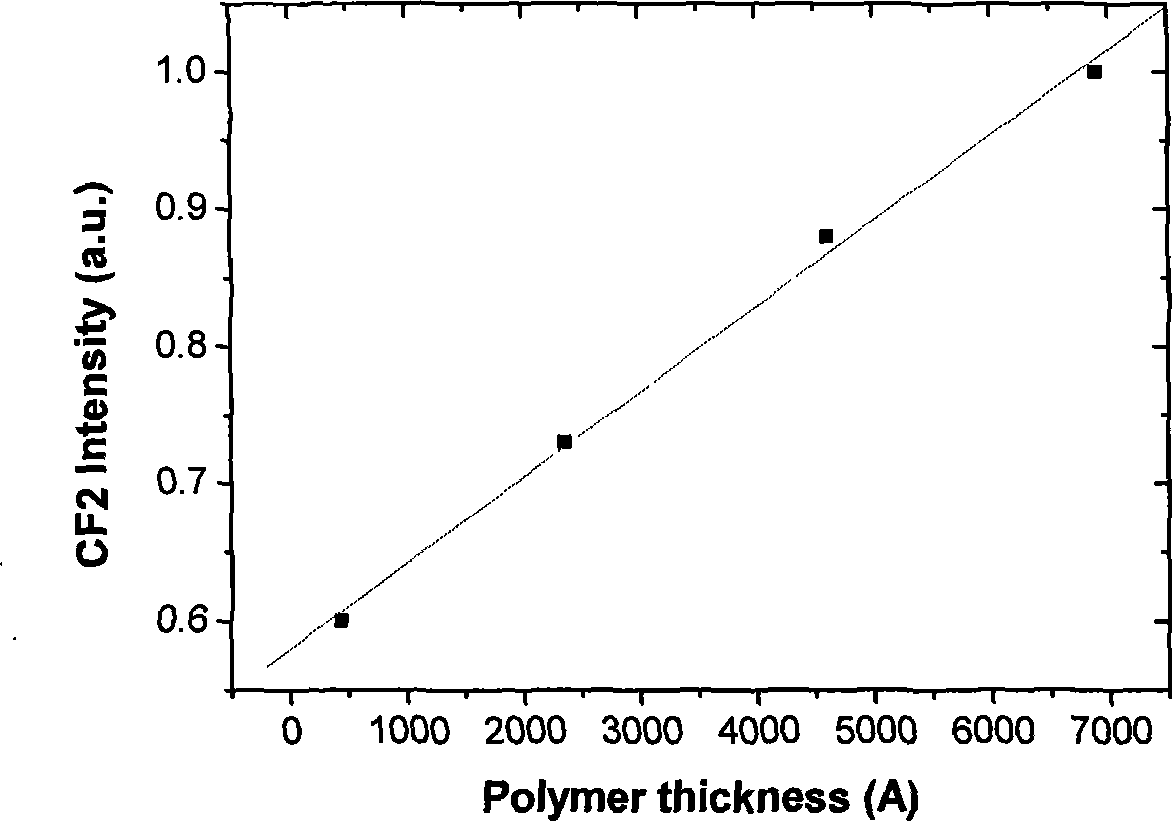
[0020] Next, the spectral signal of a specific element is screened out from the collected spectral signals of each element, wherein the intensity of the spectral signal of the specific element is linearly related to the thickness of the polymer deposited on the inner wall of the etching cavity. In this embodiment, The specified element is CF 2 ,See figure 2 , which is CF 2 Schematic diagram of the linear relationship between spectral signal intensity (Intensity) and polymer thickness (Polymer thickness).

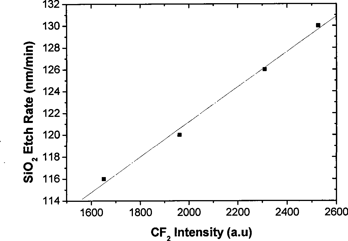
[0021] Next, according to the intens...


PUM


Abstract

The invention provides a method for monitoring an etching process by using optical emission spectroscopy characteristics, which comprises the following steps: firstly, using an optical emission spectroscopy acquiring device to acquire spectroscopy signals in real time and on line; secondly, screening spectroscopy of certain specific elements (such as CF<2>) or certain section of the spectroscopy from the spectroscopy signals, and finally determining thickness of a polymer deposited on the inner wall of a current etching chamber according to linear relation between the strength of the screened spectroscopy signals and the polymer deposited on the inner wall of the etching chamber. Therefore, the method can achieve real-time effective monitoring for an etching process.

Description

technical field [0001] The invention relates to the monitoring of a semiconductor etching process, in particular to a method for monitoring the etching process by utilizing the characteristics of optical emission spectroscopy. Background technique [0002] During the etching process of dielectric materials (such as silicon dioxide, silicon nitride, etc.), a layer of polymer is often deposited on the inner wall of the etching cavity, and its main component is CF x . The amount of this layer of polymer on the inner wall of the etching chamber will have a great impact on the characteristics of the subsequent process. For this reason, a method is needed to detect the thickness of the polymer on the inner wall of the etching chamber, and use this to judge the etching process. Whether the cavity is suitable for the requirements of the next process. [0003] In order to measure the thickness of this layer of polymer, direct measurement methods are often used nowadays, such as usi...

Claims


Application Information

Patent Timeline
Patent Type & Authority Applications(China)
IPC IPC(8): H01L21/00H01L21/66H01L21/311
Inventor 陈乐乐许昕睿林俊毅
Owner SHANGHAI HUAHONG GRACE SEMICON MFG CORP
Why Eureka
Try Eureka