Supercharge Your Innovation With Domain-Expert AI Agents!

Semiconductor device and manufacturing method thereof

A semiconductor and device technology, applied in the field of semiconductor devices and their manufacturing, can solve problems such as deteriorating device reliability, affecting wafer yield, etc., to achieve the effect of improving device performance

Inactive Publication Date: 2009-06-10
DONGBU HITEK CO LTD
View PDF2 Cites 0 Cited by
  • Summary
  • Abstract
  • Description
  • Claims
  • Application Information

AI Technical Summary

Problems solved by technology

These limitations directly and significantly impact wafer yield and can also degrade device reliability

Method used


Image

  • Semiconductor device and manufacturing method thereof
  • Semiconductor device and manufacturing method thereof
  • Semiconductor device and manufacturing method thereof

Examples


Embodiment Construction

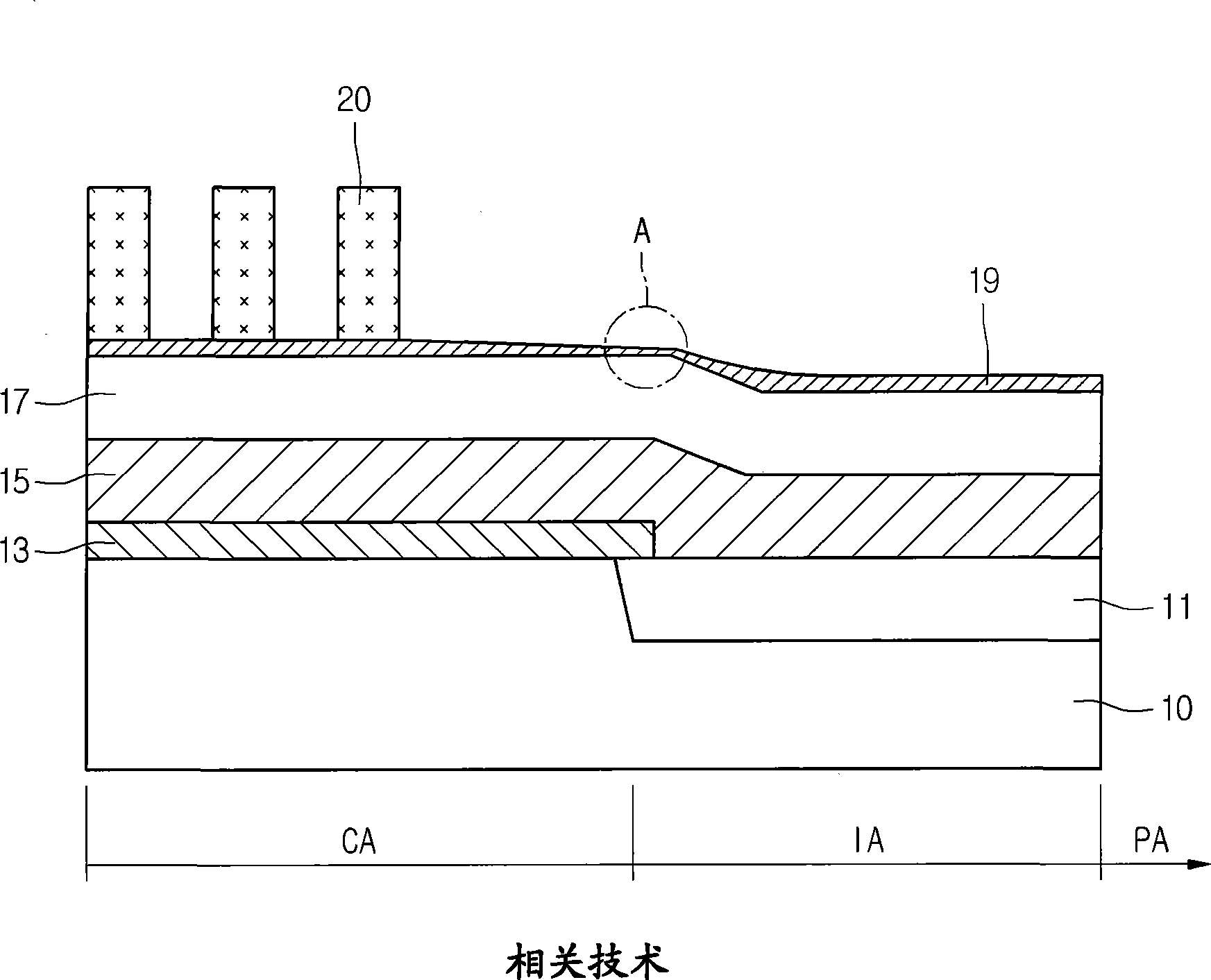
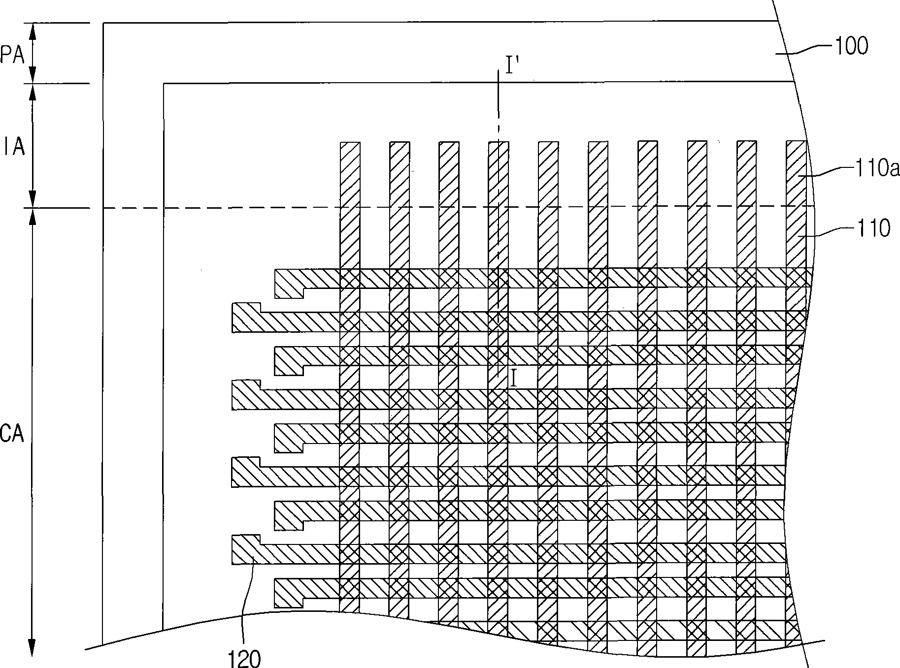
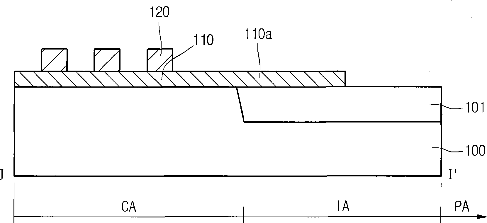
[0031] Hereinafter, a method of manufacturing a semiconductor device according to some embodiments will be described in detail with reference to the accompanying drawings. Hereinafter, components are optional or used interchangeably with each other. In the drawings, the size of each element is exaggerated to clearly illustrate that the size of each element may be different from the actual size of each element. All elements illustrated in the drawings are not necessarily included and the present disclosure is limited, but elements other than essential features of the present disclosure may be added or deleted. In the description of embodiments, it is to be understood that when a layer (or film), region, pattern or structure is referred to as being 'on / over / over' another substrate, layer (or film), region, pad or pattern, It may be directly on another substrate, layer (or film), region, pad or pattern, or intervening layers (or films), regions, pads, patterns or structures may ...


PUM


Abstract

The present invention provides a semiconductor device and a method for manufacturing the same. The semiconductor device comprises: floating grid patterns formed on unit zones of the semiconductor substrate; virtual floating grid patterns extending for the floating grid patterns to interface zones around unit zones; and control grid patterns crossing with the floating grid patterns at unit zones of the substrate.

Description

technical field [0001] The present invention relates to a semiconductor device and a method of manufacturing the same. Background technique [0002] In general, flash memory has been developed to achieve the advantages of both related art erasable programmable read only memory (EPROM) and related art electrically erasable programmable read only memory (EEPROM). The flash memory is capable of electrically programming and erasing data, and its manufacturing unit cost is relatively low due to its simple manufacturing process and miniaturized chip size. [0003] In addition, flash memory has the characteristics of random access memory (RAM), that is, flash memory is non-volatile memory that retains its stored data even when there is no power source, and can also electrically program and erase information in the system . Therefore, flash memory is often used as a storage device replacing a memory card or a hard disk of a portable electronic device. [0004] In this flash memor...

Claims


Application Information

Patent Timeline
Patent Type & Authority Applications(China)
IPC IPC(8): H01L27/115H01L21/8247H10B69/00
CPCH01L27/11548H01L27/11519H10B41/10H10B41/50H01L21/31051
Inventor 洪志镐
Owner DONGBU HITEK CO LTD
Features
  • R&D
  • Intellectual Property
  • Life Sciences
  • Materials
  • Tech Scout
  • Unparalleled Data Quality
  • Higher Quality Content
  • 60% Fewer Hallucinations
Learn More