
Thin film transistor, display device, and method for manufacturing the same
A technology for thin film transistors and a manufacturing method, which is applied in the manufacture of transistors, semiconductor/solid-state devices, and electric solid-state devices, etc., can solve the problems of complicated manufacturing processes, poor electrical properties of thin-film transistors, and reduced yield, and achieve superior electrical properties. Effect
- Summary
- Abstract
- Description
- Claims
- Application Information
AI Technical Summary
Problems solved by technology
Method used
Image

Examples
Embodiment approach 1
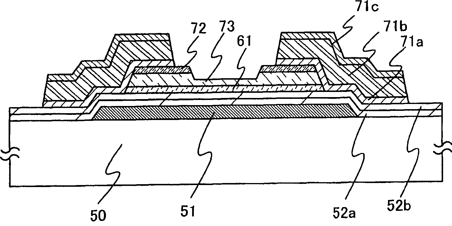
[0059] exist figure 1 In the thin film transistor shown, a gate electrode 51 is formed on a substrate 50, gate insulating films 52a and 52b are formed on the gate electrode 51, a microcrystalline germanium film 61 is formed on the gate insulating film 52b, and on the microcrystalline germanium film 61, a buffer layer 73 is formed, a pair of semiconductor films 72 added with an impurity element imparting one conductivity type are formed on the buffer layer 73, and wiring is formed on the pair of semiconductor films 72 added with an impurity element imparting one conductivity type. 71a to 71c. The microcrystalline germanium film 61 formed on the gate insulating film 52b functions as a channel formation region of the thin film transistor, and the buffer layer 73 functions as a high resistance region.
[0060] As the substrate 50, an alkali-free glass substrate such as barium borosilicate glass, aluminoborosilicate glass, aluminosilicate glass, etc., or a ceramic substrate manufa...
Embodiment approach 2
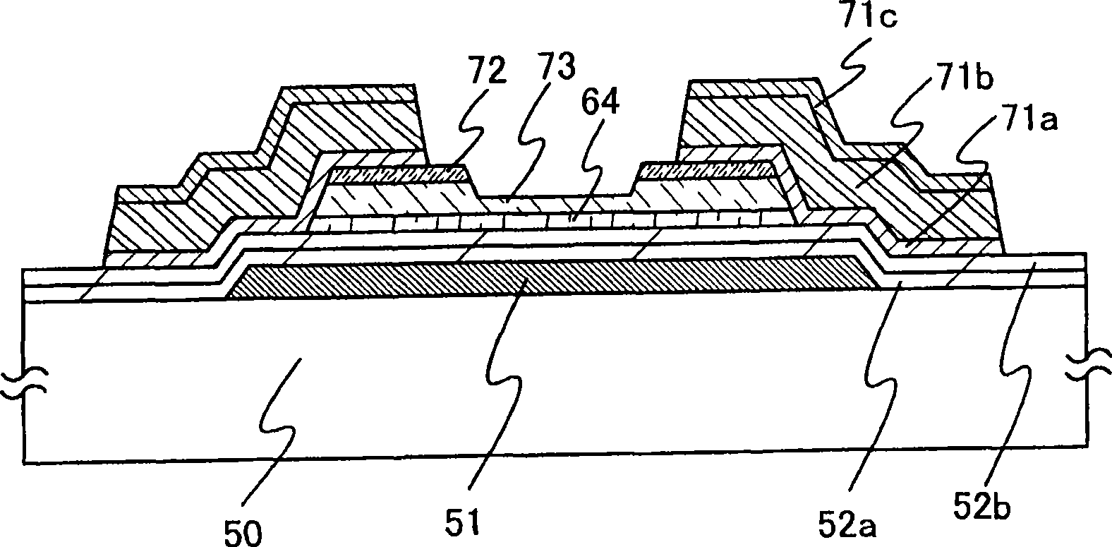
[0079] In this embodiment, refer to figure 2 A thin film transistor having a microcrystalline germanium film having a higher mobility than that of the first embodiment is shown.
[0080] exist figure 2 In the thin film transistor shown, a gate electrode 51 is formed on a substrate 50, gate insulating films 52a and 52b are formed on the gate electrode 51, and crystallites containing an impurity element serving as a donor are formed on the gate insulating film 52b. In the germanium film 64, a buffer layer 73 is formed on the microcrystalline germanium film 64 containing an impurity element serving as a donor, and a pair of semiconductor films 72 to which an impurity element imparting one conductivity type is added is formed on the buffer layer 73. Wirings 71a to 71c are formed on a pair of semiconductor films 72 having an impurity element imparting one conductivity type. Further, the microcrystalline germanium film 64 formed on the gate insulating film 52b serves as a channe...
Embodiment approach 3
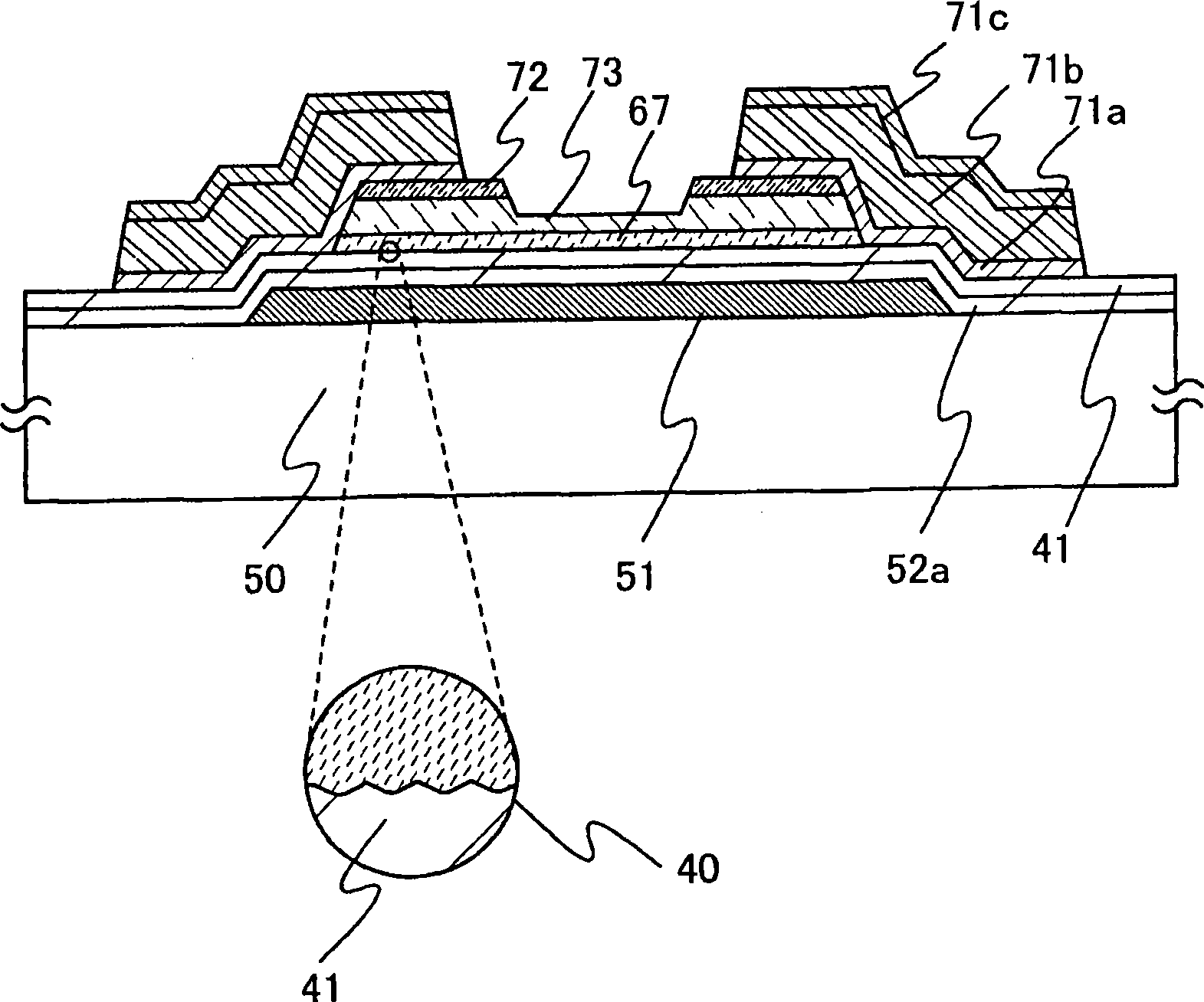
[0086] In this embodiment, refer to image 3 A thin film transistor having a microcrystalline germanium film, which has a higher field effect mobility and an improved yield compared to the first embodiment, is shown.
[0087] exist image 3 In the thin film transistor shown, a gate electrode 51 is formed on a substrate 50, a gate insulating film 52a is formed on the gate electrode 51, and a gate insulating film 41 whose surface is uneven is formed on the gate insulating film 52a. A microcrystalline germanium film 67 is formed on the gate insulating film 41, a buffer layer 73 is formed on the microcrystalline germanium film 67, and a pair of semiconductor films 72 to which an impurity element imparting one conductivity type is added is formed on the buffer layer 73. Wirings 71a to 71c are formed on a pair of semiconductor films 72 having an impurity element imparting one conductivity type. Further, the microcrystalline germanium film 67 formed on the gate insulating film 41 s...
PUM
 Abstract
Description
Claims
Application Information