Lossless absorption circuit used for inverse-excitation type switch power supply

A lossless absorption, switching power supply technology, applied in the field of circuits, can solve the problems of inconsistent conduction time requirements of the switching tube M2, nowhere to release the energy of the inductor L1, and inability to use a lossless absorption circuit, etc., to save auxiliary power, EMI interference, Loss reduction effect

Inactive Publication Date: 2009-06-10
SHANGHAI CHENRUI MICROELECTRONICS TECH
View PDF0 Cites 16 Cited by
  • Summary
  • Abstract
  • Description
  • Claims
  • Application Information

AI Technical Summary

Problems solved by technology

[0005] The lossless snubber circuit has many advantages, but it cannot be widely used at present, because its use needs to be restricted. In the previous analysis process, the voltage of capacitor C3 changes from A positive B negative to B positive A negative after the switch tube M2 is turned on. It takes a time process, which is half of the resonance period of capacitor C3 and inductor L1, and the conduction time of the switch tube is required to be greater than this time. If the switch tube cannot meet this requirement, the energy conversion between the capacitor C3 and the inductor L1 of the switch tube M2 is completed. If it is closed before, the resonant circuit of capacitor C3 and inductor L1 is closed, then the energy of inductor L1 has not been completely transferred to capacitor C3, resulting in energy accumulation in inductor L1, because the current on inductor L1 cannot be zero instantly, resulting in inductor L1 There is nowhere to release energy, and a large impact voltage will be formed on the inductor L1, which will easily cause breakdown or damage to the switch tube M2 and other devices
Since the flyback converter controls the turn-on and turn-off of the switch tube M2 through the control chip or the control circuit, when the secondary load changes, the conduction time requirements of the switch tube M2 are inconsistent, and the flyback switching power supply composed of most control chips operates in different The working process cannot fully guarantee this condition, so this lossless absorption circuit cannot be used

Method used


Image

  • Lossless absorption circuit used for inverse-excitation type switch power supply
  • Lossless absorption circuit used for inverse-excitation type switch power supply
  • Lossless absorption circuit used for inverse-excitation type switch power supply

Examples


Embodiment Construction

[0023] In order to better understand the technical solution of the present invention, it will be described in detail below through specific embodiments in conjunction with the accompanying drawings:

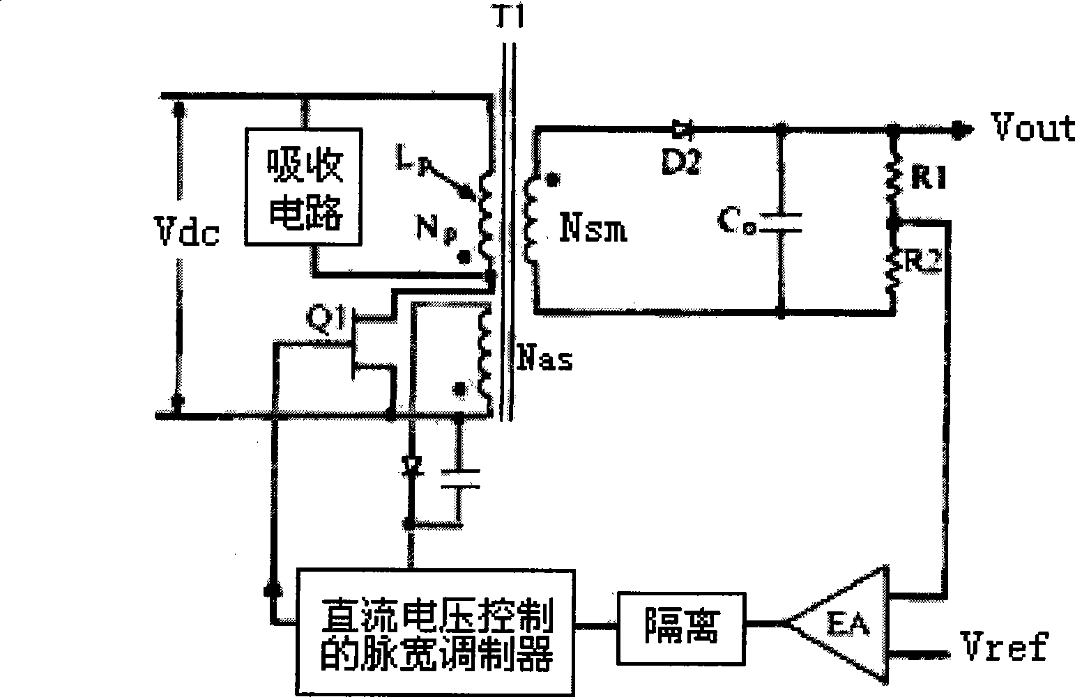
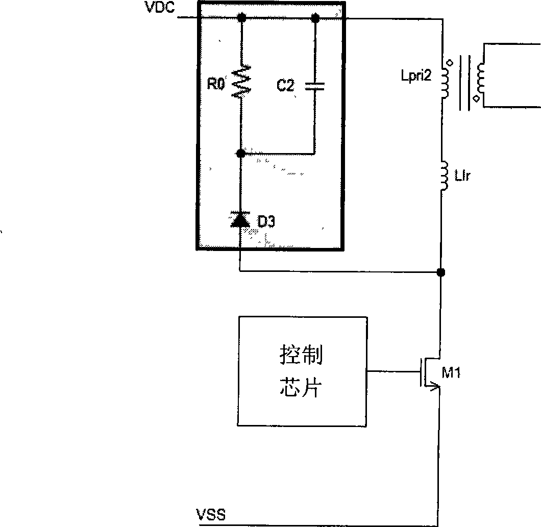
[0024] see Figure 8 , the first non-destructive snubber circuit for flyback switching power supply of the present invention, comprising a switch tube M2 connected in series with the primary coil Lpri1 of the transformer, and a switch tube M2 connected to the control pin of the switch tube M2 A working control chip, a lossless absorption circuit and a power supply circuit, wherein M2 can be a MOS tube, a triode, or other switching devices. The lossless absorption circuit consists of the first inductor LOA, the first diode D0, the second A capacitor C0 and the second diode D1 are used to absorb the peak voltage generated by the switching tube M2 at the moment of turning off. The second diode D1, the first diode D0 and the first inductor in the lossless absorption circuit LOA is s...


PUM


Abstract

The invention discloses a lossless absorber circuit for a flyback switch power, which comprises a switch tube of which the upper pin is connected in series with primary coils of a transformer, a control chip connected on the control pin of the switch tube for controlling the switch tube to work, and a lossless absorption circuit consisting of a first inductor, a first diode, a first capacitor and a second diode, and also comprises a power supply circuit consisting of the first inductor, a third diode and a second capacitor for absorbing the energy generated by the lossless absorption circuit and supplying an auxiliary power supply to the control chip. The positive terminal and the negative terminal of the third diode of the power supply circuit are connected to a node between the first inductor and the first diode in the lossless absorption circuit and the power input VDD of the control chip respectively. And the two ends of the second capacitor are connected to the power input VDD of the control chip and the negative terminal of the direct current supply respectively. The lossless absorber circuit fully uses the energy of the lossless absorber circuit, saves auxiliary power supply, and removes the limiting conditions in the application of the lossless absorber circuit.

Description

technical field [0001] The invention relates to a circuit integrating lossless absorption and auxiliary power supply for a flyback switching power supply. Background technique [0002] Basic flyback power supply circuit (see figure 1 ), in the flyback switching power supply, due to the existence of transformer leakage inductance and the influence of other distribution parameters, a large peak voltage Vclamp will be generated at the moment of turning off the switching tube Q1 during power supply operation, see figure 2 The voltage waveform of the drain of the switch tube Q1 during the turn-off process. This peak voltage Vclamp seriously threatens the normal operation of the switch tube Q1, affects the stability and safety of the entire system, and causes EMI problems. Measures must be taken to clamp or absorb it. At present, there are many ways to achieve this purpose, and the RCD absorption device is widely used because of its simple structure and low cost, such as imag...

Claims


Application Information

Patent Timeline
Patent Type & Authority Applications(China)
IPC IPC(8): H02M3/335
Inventor 喻明凡任善华林新春
Owner SHANGHAI CHENRUI MICROELECTRONICS TECH
Why Eureka
Try Eureka