Manufacturing method for mask read only memory device

A manufacturing method, mask read-only technology, applied in semiconductor/solid-state device manufacturing, electrical components, circuits, etc., to achieve the effect of reducing process complexity, avoiding mixed use of machines, and avoiding logic process incompatibility problems

Active Publication Date: 2009-06-17
SHANGHAI HUAHONG GRACE SEMICON MFG CORP
View PDF0 Cites 9 Cited by
  • Summary
  • Abstract
  • Description
  • Claims
  • Application Information

AI Technical Summary

Problems solved by technology

In this way, in the mask read-only memory manufacturing process, the problem of selective formation of metal silicide is involved

Method used


Image

  • Manufacturing method for mask read only memory device
  • Manufacturing method for mask read only memory device
  • Manufacturing method for mask read only memory device

Examples


Embodiment Construction

[0029] In order to make the technical features of the present invention more comprehensible, the present invention will be further described below in conjunction with the accompanying drawings and embodiments.

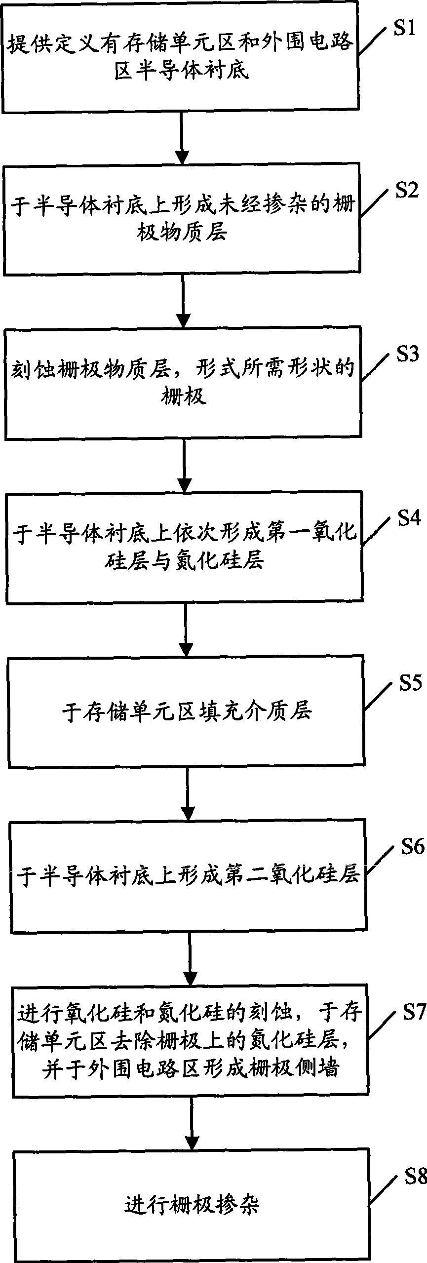
[0030] Please refer to figure 1 , which is a schematic flow chart of a mask ROM manufacturing method provided by an embodiment of the present invention. As shown in the figure, the manufacturing method of the mask ROM includes the following steps:

[0031] S1: Provide a semiconductor substrate defined with a memory cell area and a peripheral circuit area;

[0032] S2: forming an undoped gate substance layer on the semiconductor substrate;

[0033] S3: Etching the gate material layer to form a gate with a desired shape;

[0034] S4: sequentially forming a first silicon oxide layer and a silicon nitride layer on the semiconductor substrate;

[0035] S5: filling the medium layer in the storage unit area;

[0036] S6: forming a second silicon oxide layer on the semico...


PUM

PropertyMeasurementUnit
Thicknessaaaaaaaaaa
Thicknessaaaaaaaaaa
Thicknessaaaaaaaaaa

Abstract

The invention discloses a method of manufacturing masked read-only memories, which includes steps of providing a semiconductor substrate defined with a memory cell region and a peripheral circuit region, forming an undoped gate material layer on the semiconductor substrate, etching the gate material layer to form a gate in required shape, sequentially forming a first silicon oxide layer and a silicon nitride layer on the semiconductor substrate, filling a dielectric layer in the memory cell region, forming a second silicon oxide layer on the semiconductor substrate, performing silicon oxide and silicon nitride etching, removing the silicon nitride layer from the gate of the memory cell region and forming gate sidewalls at the peripheral circuit region, and performing gate doping. Therefore, the method adopts the undoped gate material layer to form the gate, and the technological process is compatible with standard CMOS technique, thereby avoiding logical process incompatibility caused by the preliminarily doped gate material layer.

Description

technical field [0001] The invention relates to a manufacturing method of a semiconductor storage device, in particular to a manufacturing method of a mask read-only memory (MROM). Background technique [0002] Mask read-only memory (MROM) is one of the common types of semiconductor memory, which is widely used in electronic products such as computers. The mask read-only memory is composed of a memory cell array and a peripheral logic circuit. The memory cell array is usually composed of mutually orthogonal bit lines and word lines: the embedded layer is formed in the memory cell area by ion implantation technology, and the bit line can be formed by further heat treatment. Lines, and word lines are usually gate structures, which are formed through photolithography and etching processes; and peripheral logic circuits often include multiple logic transistors. In the existing mask read-only memory manufacturing process, the gate structure of the logic transistor of the periphe...

Claims


Application Information

Patent Timeline
IPC IPC(8): H01L21/8246
Inventor 李栋徐爱斌李荣林董耀旗孔蔚然
Owner SHANGHAI HUAHONG GRACE SEMICON MFG CORP
Why Eureka
Try Eureka