FD active region structure for pixel unit, preparation and CMOS image sensor thereof
A pixel unit and active area technology, applied in the field of image sensors, can solve problems such as image distortion, unsatisfactory camera image clarity, large leakage current in FD active area, etc., to eliminate dark current, ensure clarity, reduce The effect of dark current
- Summary
- Abstract
- Description
- Claims
- Application Information
AI Technical Summary
Problems solved by technology
Method used
Image

Examples
Example Embodiment
[0036] Example one
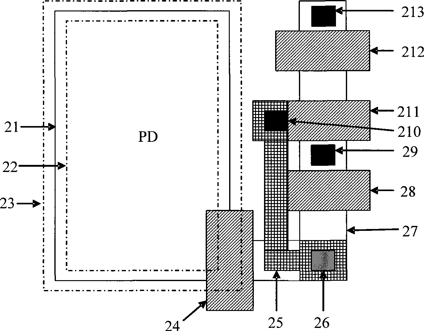
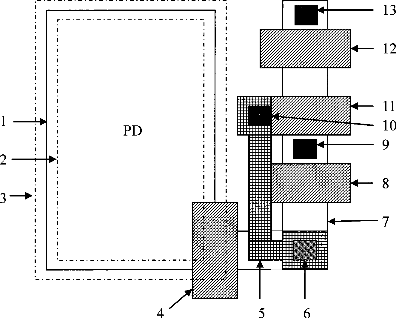
[0037] This embodiment provides an FD active area structure of a pixel unit, such as image 3 , Figure 7-9 As shown, specifically including:
[0038] A P-type well (ie: P-type silicon semiconductor well) is formed on the P-type silicon semiconductor substrate, and an N-type silicon semiconductor injection layer is arranged on the P-type well to form the FD active area of the pixel unit. The semiconductor implantation layer also includes an N-Plus ion implantation layer, and a P-type silicon semiconductor implantation layer is provided around the N-type silicon semiconductor implantation layer. The P-type silicon semiconductor implantation layer and the N-type silicon semiconductor implantation layer form the opposite To the PN junction, it is used to isolate the N-type silicon semiconductor injection layer from the shallow trench isolation area STI (Shallow Trench Isolation) of the device. The N-type silicon semiconductor injection layer is provided with a P...
Example Embodiment
[0056] Example two
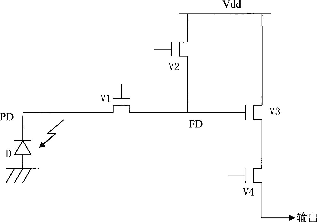
[0057] This embodiment provides a CMOS image sensor. The structure of the CMOS image sensor is basically the same as that of the existing CMOS image sensor. A plurality of pixel units can be connected to form a pixel array. Each pixel unit is composed of a photodiode, a transmission gate tube, and a reset tube. The difference between the source follower tube and the strobe tube and the existing CMOS image sensor is that the FD active area connected to the transmission gate tube, reset tube, and source follower tube in each pixel unit of the CMOS image sensor adopts the first embodiment described above. Any FD active area structure given in this can ensure that the leakage current of the pixel unit is reduced when working in the global exposure mode, thereby ensuring the clarity of the CMOS image sensor when shooting high-speed moving objects.
[0058]In summary, in the embodiment of the present invention, by improving the layout structure and process of the FD...
PUM
| Property | Measurement | Unit |
|---|---|---|
| Channel length | aaaaa | aaaaa |
Abstract
Description
Claims
Application Information
 - Generate Ideas
- Intellectual Property
- Life Sciences
- Materials
- Tech Scout
- Unparalleled Data Quality
- Higher Quality Content
- 60% Fewer Hallucinations
Browse by: Latest US Patents, China's latest patents, Technical Efficacy Thesaurus, Application Domain, Technology Topic, Popular Technical Reports.
© 2025 PatSnap. All rights reserved.Legal|Privacy policy|Modern Slavery Act Transparency Statement|Sitemap|About US| Contact US: help@patsnap.com