Thin film photovoltaic structure and fabrication

A photovoltaic and structural technology, used in semiconductor/solid-state device manufacturing, semiconductor devices, electrical components, etc., can solve problems affecting photovoltaic cell performance, photovoltaic structure cost suppression, etc., to achieve high manufacturing volume, improve manufacturing yield, and low cost. Effect

Inactive Publication Date: 2009-06-24
CORNING INC
View PDF2 Cites 8 Cited by
  • Summary
  • Abstract
  • Description
  • Claims
  • Application Information

AI Technical Summary

Problems solved by technology

[0011] In contrast to microelectronic applications of SOI structures, photovoltaic structures are more tolerant of such defects, although such defects can still adversely affect the performance of photovoltaic cells
While such trimming techniques like CMP improve surface properties, the defect tolerance of photovoltaic structures keeps their cost prohibitive

Method used


Image

  • Thin film photovoltaic structure and fabrication
  • Thin film photovoltaic structure and fabrication
  • Thin film photovoltaic structure and fabrication

Examples


Embodiment Construction

[0040] Unless otherwise indicated, all numbers used in the specification and claims, such as those expressing weight percentages of ingredients, dimensions and values ​​of certain physical properties, are to be understood in all instances to be preceded by the term "about" grooming. It should also be understood that the precise numerical values ​​used in the specification and claims constitute additional embodiments of the invention. Efforts have been made by the inventors to ensure the accuracy of the numerical values ​​disclosed in the examples. Any measured numerical value, however, inherently contains certain errors resulting from the standard deviation found in the respective measurement technique.

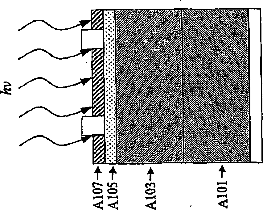
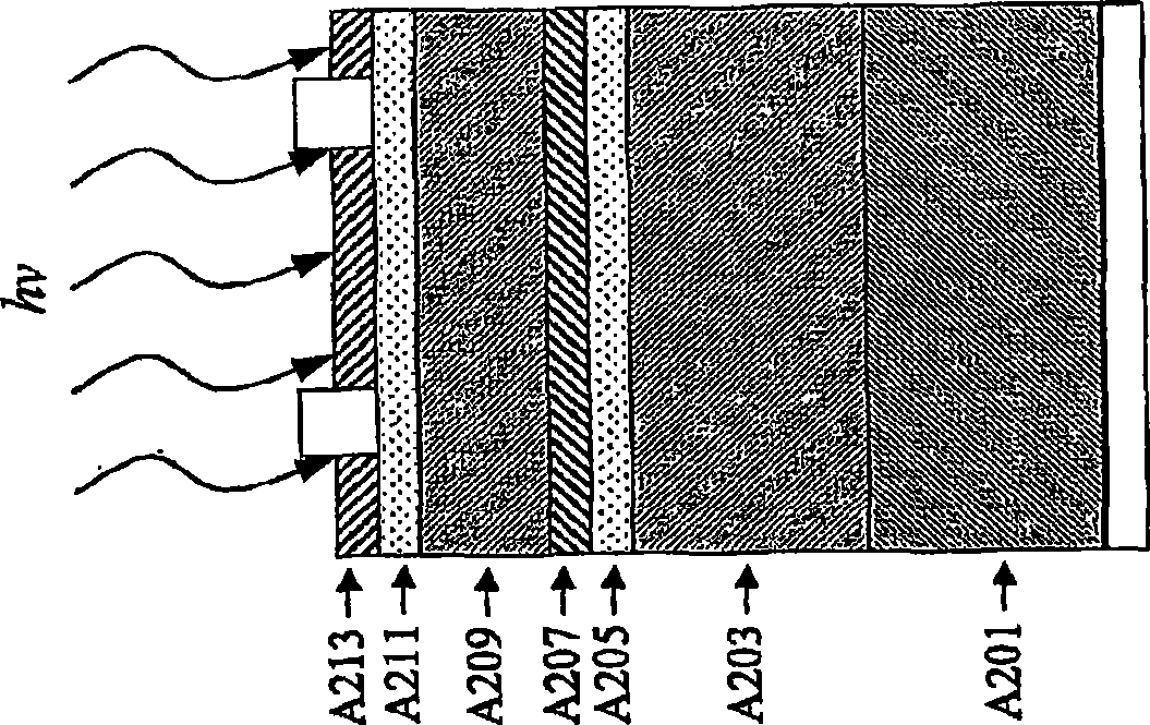
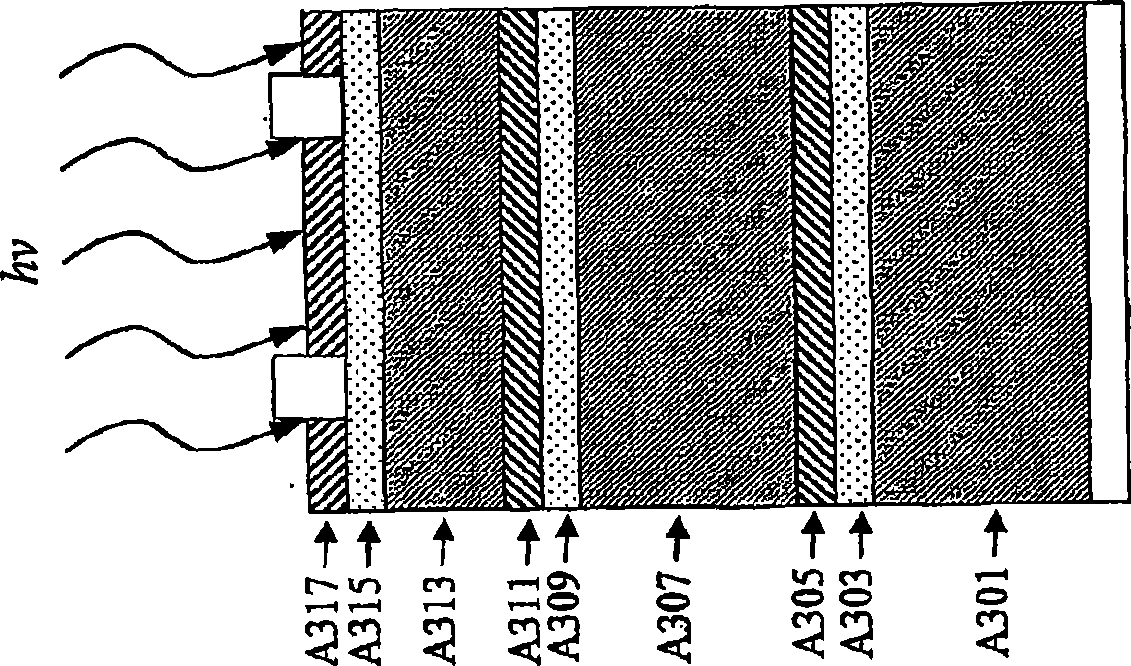
[0041] By "crystalline semiconductor material" it is meant that the material may be entirely crystalline or substantially crystalline, with or without defects and / or dopants introduced intentionally or accidentally. It shall therefore include: (i) precursor materials used t...


PUM

PropertyMeasurementUnit
band gapaaaaaaaaaa
strain pointaaaaaaaaaa
thicknessaaaaaaaaaa

Abstract

Novel photovoltaic structures comprising an insulator structure bonded to an exfoliation layer, preferably of a substantially single-crystal donor semiconductor wafer, and at least one photovoltaic device layer, such as a conductive layer, and systems and methods of production of a photovoltaic device, comprising creating on a donor semiconductor wafer an exfoliation layer and transferring the exfoliation layer to an insulator substrate.

Description

technical field [0001] The present invention relates to systems, methods and products for producing thin film photovoltaic structures, preferably having thin films that are substantially single crystal, and utilizing improved processes comprising: transferring a base of a photovoltaic structure or a partially completed photovoltaic structure to an insulator substrate, and anodically bonded to the insulator substrate. Background technique [0002] Photovoltaic structures (PVS) are special forms of semiconductor structures that convert photons into electricity. Fundamentally, the device needs to fulfill two functions: the photogeneration of charge carriers (electrons and holes) in the light-absorbing material, and the separation of the charge carriers to the conductive contacts that will carry the current. This conversion is called the photovoltaic (PV) effect, and is used in solar cells, which convert light energy into electrical energy, and the field of research on solar ce...

Claims


Application Information

Patent Timeline
Patent Type & Authority Applications(China)
IPC IPC(8): H01L21/84H01L21/762C03C27/02H01L31/0392H01L31/18
Inventor D·F·道森一埃利K·P·加德卡尔R·M·沃尔顿
Owner CORNING INC
Why Eureka
Try Eureka