
Power diode with trench field ring structure

A technology for power semiconductors and semiconductors, which is applied in the fields of semiconductor devices, semiconductor/solid-state device manufacturing, electrical components, etc., and can solve the problems of heavy metal pollution in the diffusion area and long diffusion time of dopants.

Inactive Publication Date: 2009-07-15
SEMIKRON ELECTRONICS GMBH & CO KG
View PDF0 Cites 2 Cited by
  • Summary
  • Abstract
  • Description
  • Claims
  • Application Information

AI Technical Summary

Problems solved by technology

[0003]Because here the deep diffusion of dopants requires very long diffusion times and thus there is a risk that the diffusion zone will be contaminated, for example with heavy metals

Method used


Image

  • Power diode with trench field ring structure
  • Power diode with trench field ring structure
  • Power diode with trench field ring structure

Examples


Embodiment Construction

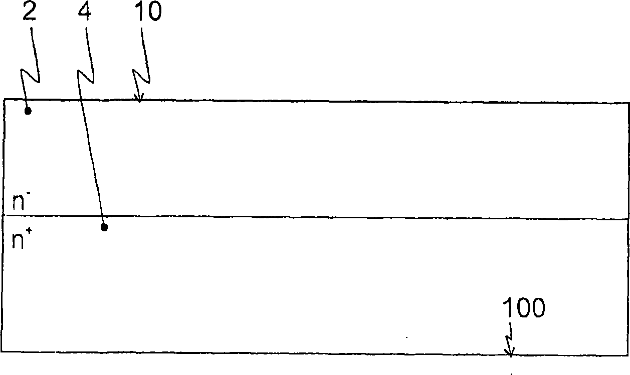
[0023] figure 1 Using the example of a power diode with a reverse voltage of 1200 V, parts of the base body 2 , 4 of the power semiconductor component according to the invention are shown not to scale. This example also applies in principle to the subsequent figures. In this case, the semiconductor body has two different concentrations of n-doping. Adjacent to the first surface 10 of the base body is a weakly doped region 2 , and adjoining the second surface 100 is a heavily doped region 4 . The boundaries of the two dopants run parallel to the surfaces 10 , 100 in the interior of the matrix.

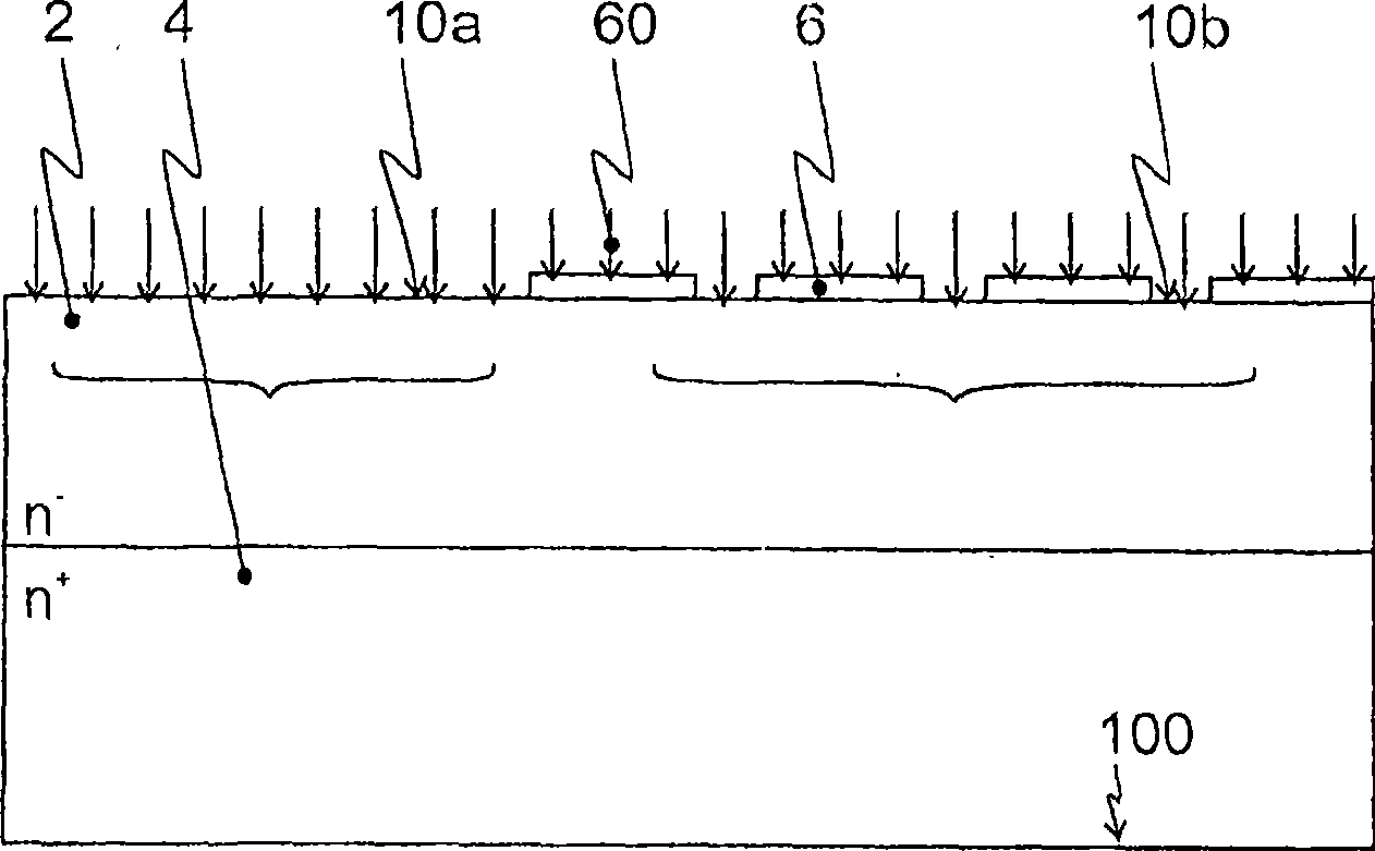
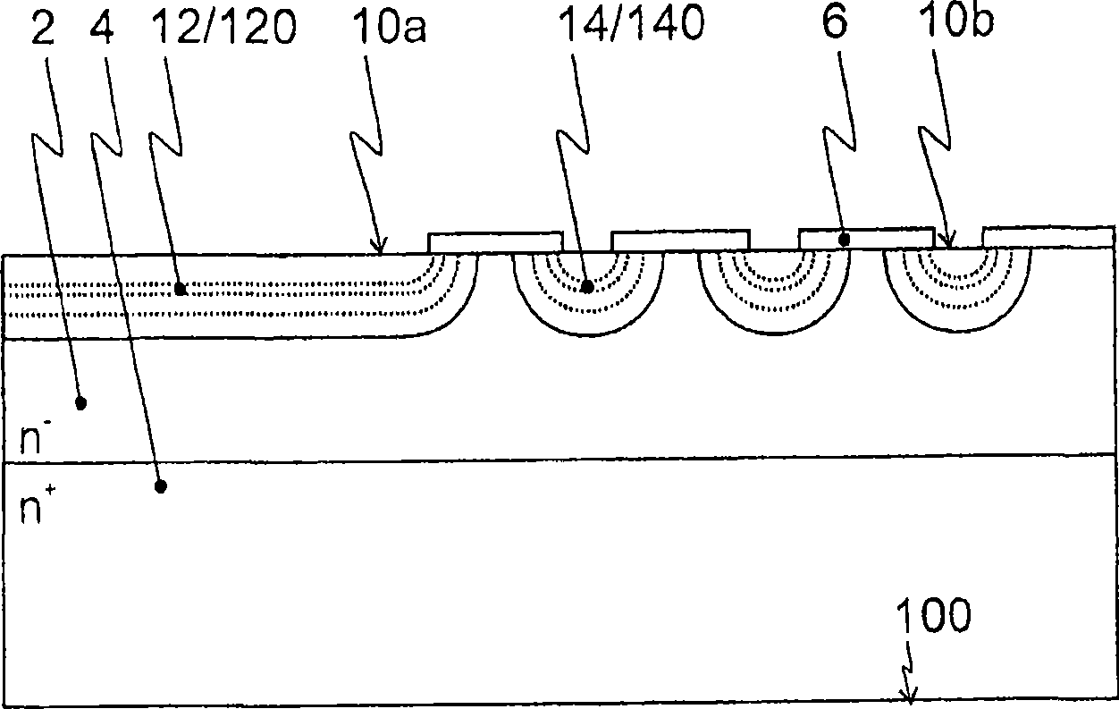
[0024] figure 2 Partial steps of a first method for forming a second doped doping profile both for the contact region and for the field ring structure are shown. According to the prior art, the different regions are here masked 6 in order to provide selective doping. The contact region is formed in the region of the first partial surface 10 a and the field ring of the field ring ...


PUM


Abstract

The invention relates to a power semiconductor component comprising a semiconductor base body having a first doping and a method of producing the same. In the base body having the first doping, a pn junction is formed by means of a contact region having a second doping with a first doping profile. A field ring structure having a second doping with a second doping profile of the respective field ring is likewise arranged. In this case, the contact region and the field ring structure are arranged at respectively assigned first and second partial areas of a first surface of the base body. Both the contact region and the field ring structure extend into the volume of the base body, wherein the base body has, for the field ring structure, a trench-type cutout assigned to the respective field ring, the surface of the cutout essentially following the contour of the assigned doping profile, the depth extent of the trenches in the contact region and the field ring structure is a maximum of about 90 percent and a minimum of about 50 percent of the penetration depth of the second doping, and the penetration depth of the second doping is between about 10 [mu]m and about 30 [mu]m.

Description

technical field [0001] The invention describes a power semiconductor component having at least one pn junction, preferably a power diode with a reverse voltage strength of at least 600V, for use in a power stage converter. The main requirement for such power semiconductor components is therefore the edge region which contributes to this reverse voltage strength. Background technique [0002] According to the prior art, in order to meet this requirement it is known to arrange a concentric structure consisting of a plurality of field rings in the edge region of the power semiconductor component. In this case, it is known that such field rings are produced by a diffusion process in which a mask of dopant is applied to the surface and then diffuses into the semiconductor as a result of the temperature action, whereby the diffusion profile is formed. For power semiconductor components capable of bulk conduction, field rings are usually formed in this case together with the creat...

Claims


Application Information

Patent Timeline
Patent Type & Authority Applications(China)
IPC IPC(8): H01L29/861H01L29/06H01L21/329
CPCH01L29/8611H01L29/66128H01L29/417
Inventor B·柯尼希
Owner SEMIKRON ELECTRONICS GMBH & CO KG
Learn More