Semiconductor encapsulation structure having substrate identification code and manufacturing method thereof

A manufacturing method, semiconductor technology, applied in semiconductor/solid-state device manufacturing, semiconductor devices, semiconductor/solid-state device components, etc.

Inactive Publication Date: 2009-07-22
POWERTECH TECHNOLOGY
View PDF1 Cites 15 Cited by
  • Summary
  • Abstract
  • Description
  • Claims
  • Application Information

AI Technical Summary

Problems solved by technology

[0006] Another object of the present invention is to overcome the defects existing in the substrate identification code of the existing semiconductor package structure, and provide a new semiconductor package structure with a substrate identification code and its manufacturing method. The technical problem to be solved is in the laser There is no need to adjust the laser light or change the laser marking mach

Method used


Image

  • Semiconductor encapsulation structure having substrate identification code and manufacturing method thereof
  • Semiconductor encapsulation structure having substrate identification code and manufacturing method thereof
  • Semiconductor encapsulation structure having substrate identification code and manufacturing method thereof

Examples


Embodiment Construction

[0067] In order to further explain the technical means adopted by the present invention to achieve the intended purpose of the invention, the specific implementation methods, The structure, manufacturing method, steps, features and functions thereof are described in detail below. For convenience of description, in the following embodiments, the same elements are denoted by the same numbers.

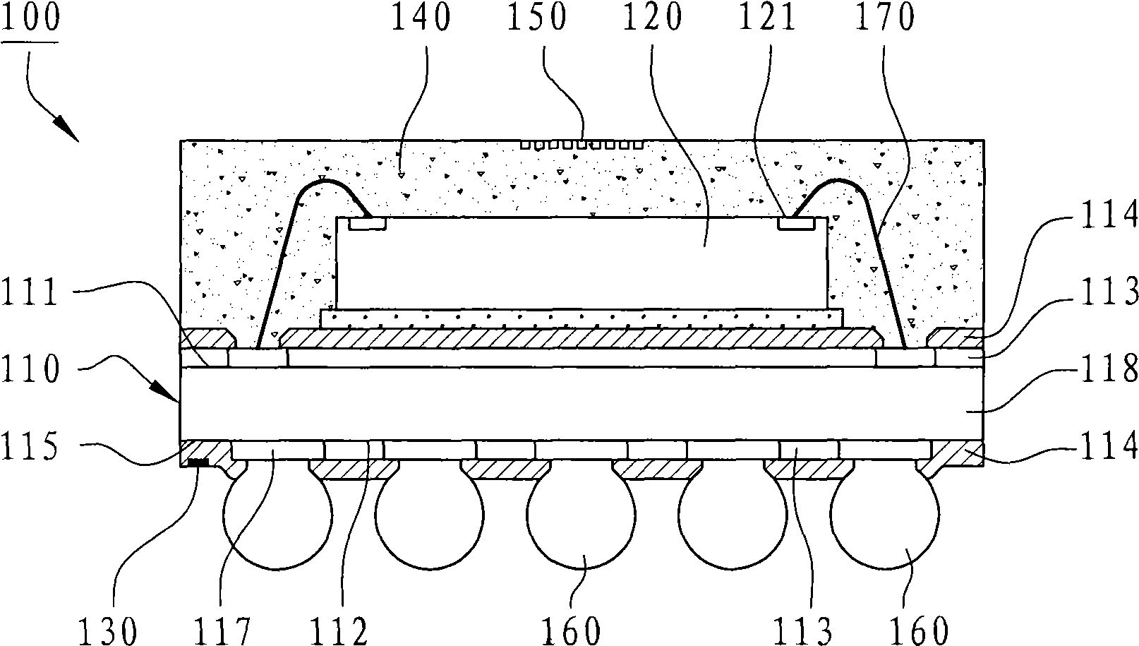
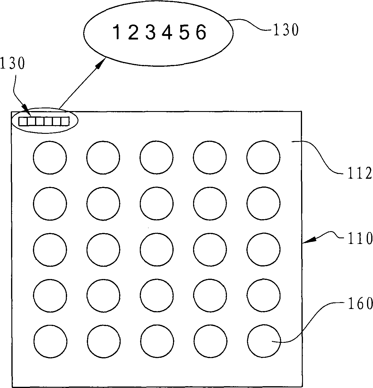
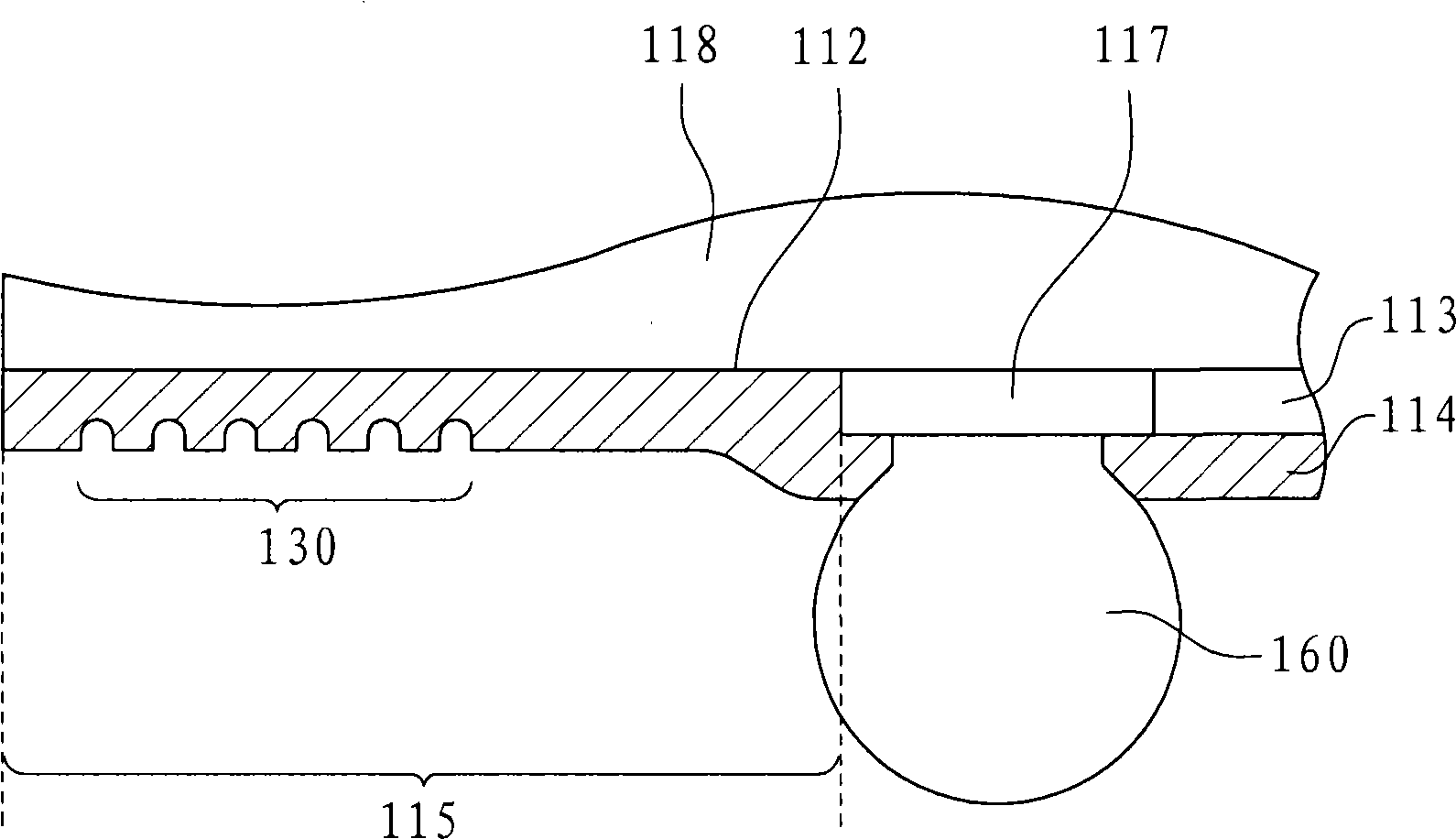
[0068] According to the first specific embodiment of the present invention, a semiconductor package structure with a substrate identification code and its manufacturing method, refer to Figure 1 to Figure 6 described as follows. see figure 1 As shown, a semiconductor package structure 100 mainly includes a substrate 110 , a chip 120 and a substrate identification code 130 . Wherein, the substrate 110 has an upper surface 111 and a lower surface 112 . The substrate 110 serves as a chip carrier and has a single-layer or multi-layer circuit structure. In this embodiment, the upper surf...


PUM


Abstract

The invention relates to a semiconductor encapsulation construct with a base plate identification code and a manufacturing method thereof. The lower surface of a base plate is formed with a circuit layer and a welding cover layer which roughly covers the circuit layer and a non circuit area. A wafer is arranged on the upper surface of the base plate. The base plate identification code escapes the circuit layer, is formed on the welding cover layer of the base plate or an adhesive body by laser marking and is used for marking product batch of the base plate. Therefore, the product batch can be traced by the encapsulation construct, and the encapsulation construct can be used for quality control and abnormal tracing while the appearance is not needed to be changed. In addition, the base plate identification code can be formed by utilizing the existing laser marking board for semiconductor encapsulation and the laser marking, thus being convenient for manufacture and not damaging the circuit layer of the base plate.

Description

technical field [0001] The invention relates to a semiconductor device, in particular to a semiconductor packaging structure with a substrate identification code and a manufacturing method thereof. Background technique [0002] In the semiconductor packaging process, substrate strips (or called array packaging substrates or motherboards) are used as structural components, which are composed of multiple substrate units arranged in a matrix, and the number can range from tens to hundreds. many. After the semiconductor package is completed, the array substrates are cut to form independent chip package structures. In order to do follow-up production management, quality control and product tracking, a substrate identification mark will be made on the substrate for management. However, the conventional substrate identification mark is formed in the substrate process, which increases the manufacturing cost and is covered or cut off in the semiconductor packaging process. [0003...

Claims


Application Information

Patent Timeline
IPC IPC(8): H01L23/544H01L23/498H01L21/00H01L21/48H01L21/50
CPCH01L2924/15311H01L2224/4824H01L2924/15151H01L2223/54433H01L2224/73265H01L2924/3025H01L2224/48227H01L2224/73215H01L2224/32225H01L24/73H01L2924/14H01L2924/181H01L2924/00012H01L2924/00
Inventor 陈锦弟洪菁蔚余秉勋王进发
Owner POWERTECH TECHNOLOGY
Why Eureka
Try Eureka