
Eureka
For R&D, Eureka makes reading and utilizing patents & technical documents easy.
Eureka AIR
Designed for self-driven R&D workflows. Generate viable solutions, solve complex R&D challenges, empower your innovation with AI.

Eureka Materials
Designed for material experts only. Revolutionize your material R&D, from search, analyze, to developing new materials.

TechResearch
Generate reliable direction feasibility study reports for your R&D in just a few steps.

TechSeek
Discover and master advanced knowledge NOW. Basics, ideas, possibilities, all at once.

TechMind
As an expert in R&D Theories, TechMind can generates customized viable solutions instantly.

TechRisk
Analyze your overall solution with one click, know your potential R&D risks in advance.

TechMonitor
Get weekly tech updates, stay abreast of the latest tech innovations and key insights.
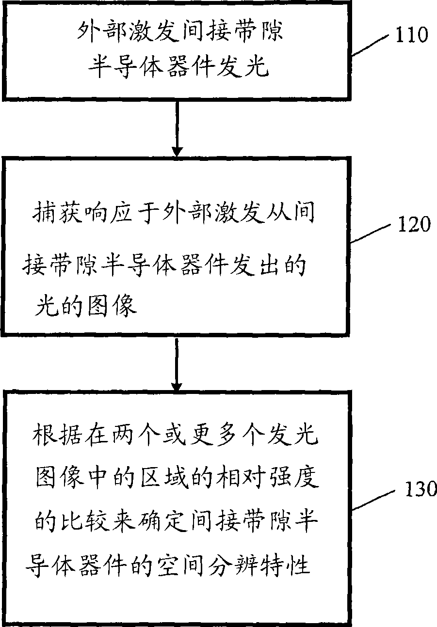
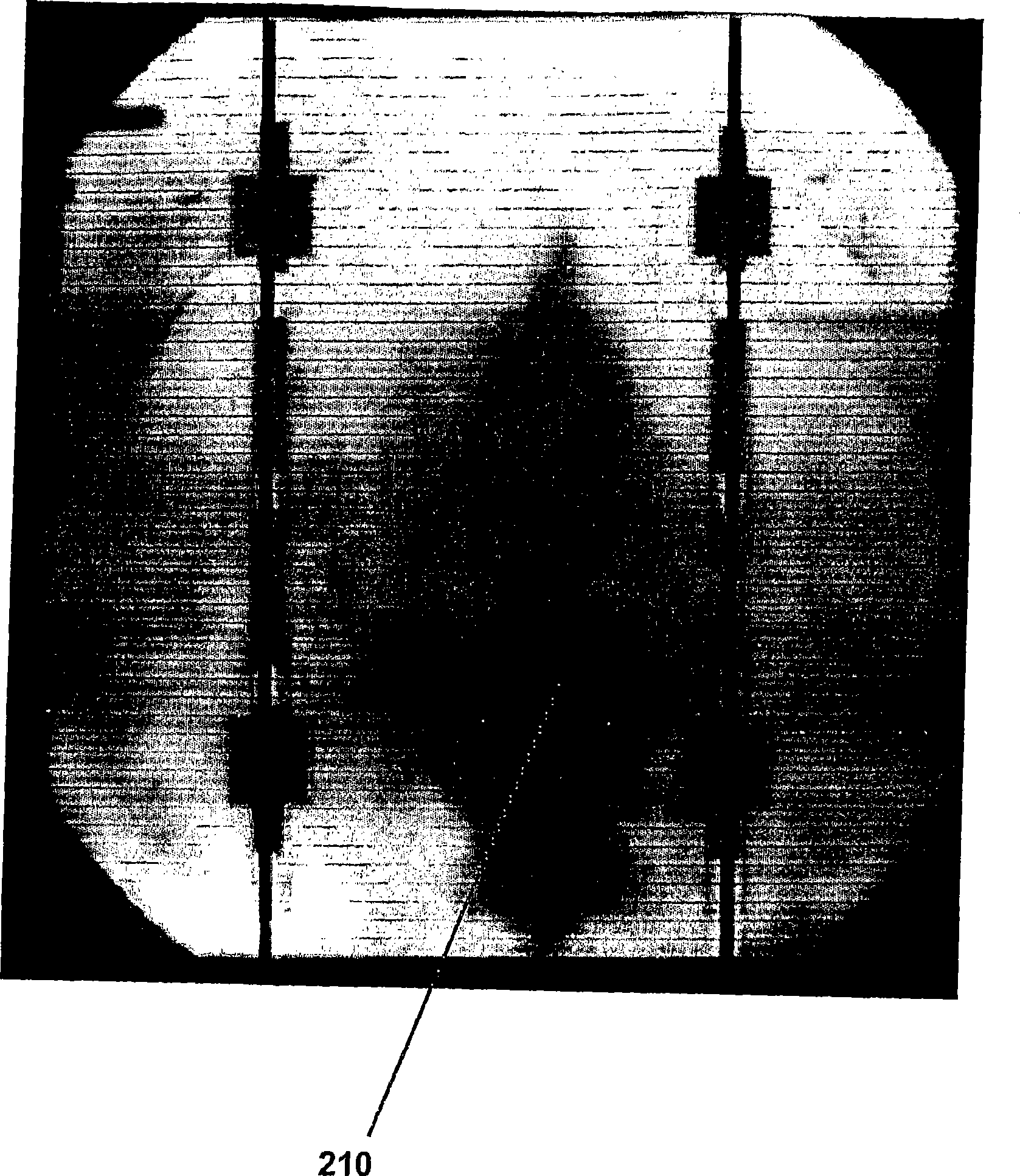
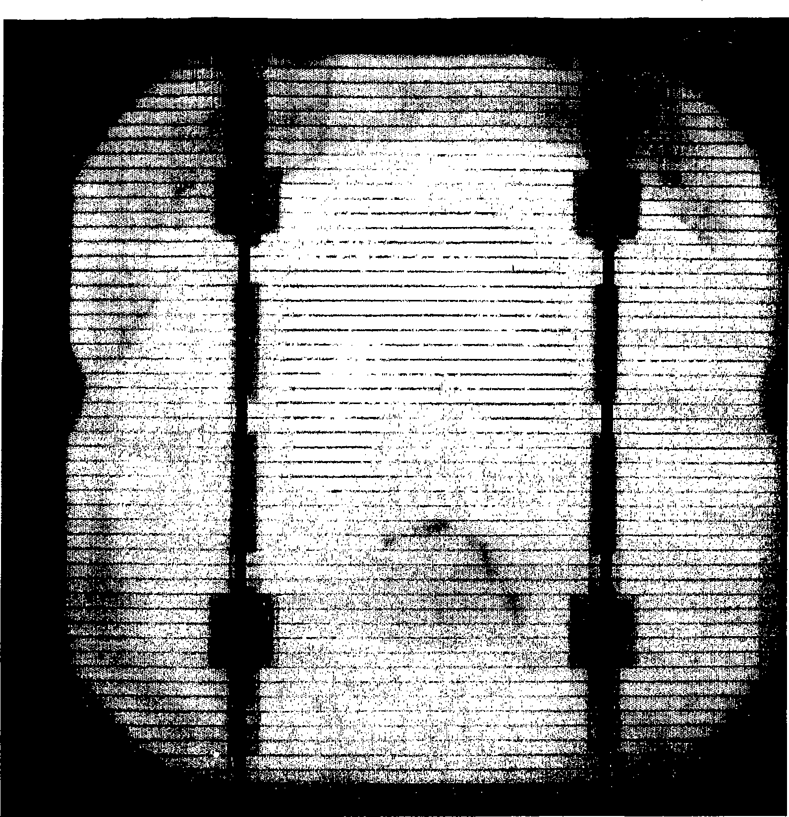
Method and system for testing indirect bandgap semiconductor devices using luminescence imaging
A technology of semiconductor and light-emitting images, which is applied in semiconductor devices, semiconductor/solid-state device testing/measurement, photometry, etc., and can solve problems such as reducing the efficiency of solar cells
- Summary
- Abstract
- Description
- Claims
- Application Information
AI Technical Summary
Problems solved by technology
Method used
Image

Examples
Embodiment Construction
[0030] Embodiments of methods and systems for electroluminescent and photoluminescent imaging of indirect bandgap semiconductor devices are described below. Although certain embodiments have been described with specific reference to solar cells, it is not intended that the invention be limited to such devices, as the principles of the invention have general applicability to optoelectronic devices and / or semiconductor devices and structures, which may all or partially processed.
[0031] In the context of this specification, references to electrically isolated or poorly connected areas are intended to include partially electrically isolated areas within the intended meaning. For example, electrically isolated or poorly connected regions include regions that resistively couple to other regions.
[0032] The methods used to optically inspect or test indirect bandgap semiconductor devices such as optoelectronic devices and solar cells differ in the way the devices are excited. I...
PUM
 Abstract
Description
Claims
Application Information
 - R&D Engineer
- R&D Manager
- IP Professional
- Industry Leading Data Capabilities
- Powerful AI technology
- Patent DNA Extraction
Browse by: Latest US Patents, China's latest patents, Technical Efficacy Thesaurus, Application Domain, Technology Topic, Popular Technical Reports.
© 2024 PatSnap. All rights reserved.Legal|Privacy policy|Modern Slavery Act Transparency Statement|Sitemap|About US| Contact US: help@patsnap.com