System and method for electric test of semiconductor wafer

一种半导体、电测试的技术,应用在电子电路测试、非接触式电路测试、单个半导体器件测试等方向,能够解决影响集成电路电特征等问题,达到消除干扰的效果

Inactive Publication Date: 2009-08-05
APPL MATERIALS ISRAEL LTD
View PDF1 Cites 16 Cited by
  • Summary
  • Abstract
  • Description
  • Claims
  • Application Information

AI Technical Summary

Problems solved by technology

[0005] Fabrication failures can affect the electrical characteristics of integrated circuits

Method used


Image

  • System and method for electric test of semiconductor wafer
  • System and method for electric test of semiconductor wafer
  • System and method for electric test of semiconductor wafer

Examples


Embodiment Construction

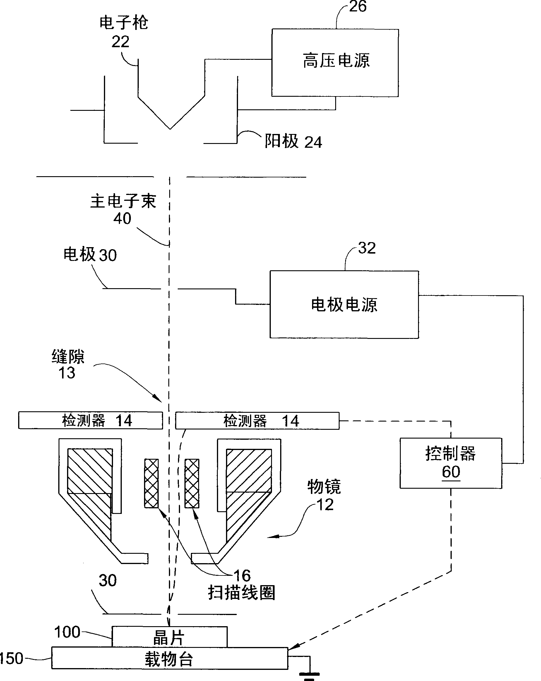
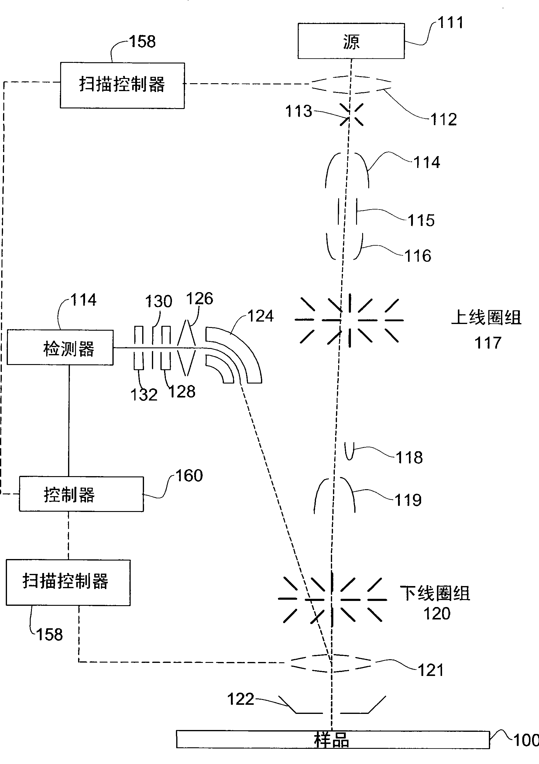
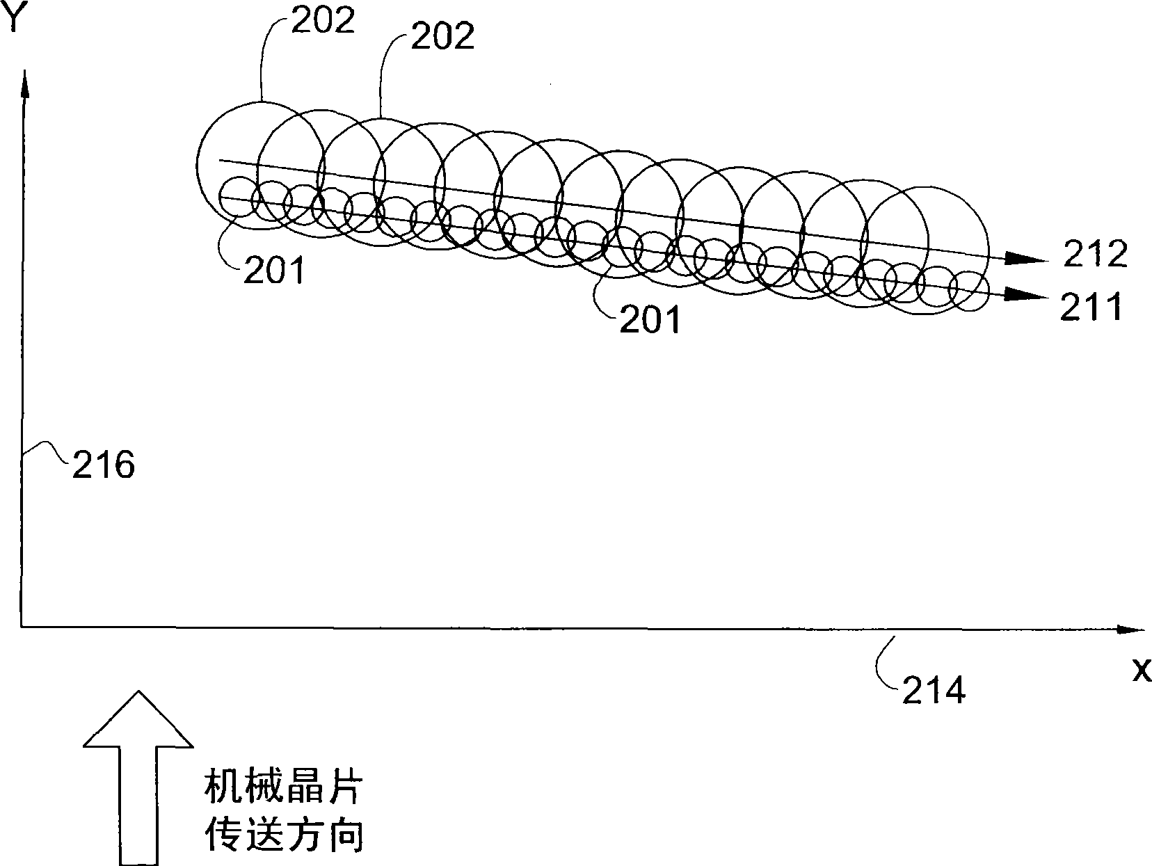
[0059] The following description relates to charged particle microscopes, such as scanning electron microscopes (SEM), especially step and repeat type SEMs. In charged particle microscopes, it is usually done by scanning an area of ​​the wafer (determined by the field of view of the SEM). Area) and mechanically introduce relative motion between the wafer and the SEM to advance the repeated steps of scanning another area to scan the wafer. For example, the relative movement can be achieved by an electrostatic field and / or a magnetic field introduced by different electrostatic and / or magnetic elements such as lenses, deflectors, etc. It should be pointed out that other charged particles and even photons can be used to detect voltage contrast. It should also be pointed out that the present invention can also be implemented by introducing a substantially constant movement between the SEM and the wafer. The relative movement can be linear or even rotational, and / or any combination of t...


PUM


Abstract

A system for electrically testing a semiconductor wafer, the system including (a) at least one charged particle beam focus effecting component and (b) at least one detector adapted to collect charged particles scattered from the wafer; wherein the system is adapted to scan a first area of a sample by a de-focused charged particle beam so as to affect a charging of the first area, scan at least a portion of the first area by a focused charged particle beam and detect electrons scattered from the at least portion. The system scans the at least portion while the first area remains affected by the de-focused charged particle beam. A method for electrically testing a semiconductor wafer includes scanning a first area of a sample by a de-focused charged particle beam so as to affect a charging of the first area; and scanning at least a portion of the first area by a focused charged particle beam while detecting electrons scattered from the at least portion, the at least portion being scanned while the first area remains affected by charging introduced by the de-focused charged particle beam.

Description

Technical field [0001] The present invention relates to an apparatus and method for inspecting and testing semiconductor wafers during circuit manufacturing, especially for testing wafers in voltage contrast mode. Background technique [0002] Integrated circuits are very complex devices that include multiple layers. Each layer may include conductive materials, insulating materials, and / or semiconductor materials. These various materials are usually arranged in patterns according to the expected functionality of the integrated circuit. The pattern also reflects the manufacturing process of the integrated circuit. [0003] The conductive layer usually includes some conductors made of conductive materials separated by insulating materials such as various oxides. The dielectric layers are arranged between the conductive layers in a staggered manner. The conductors of different conductive layers can be connected to each other and / or to the substrate by conductive materials (referred ...

Claims


Application Information

Patent Timeline
Patent Type & Authority Applications(China)
IPC IPC(8): H01L21/66G01R31/265G01R31/28
CPCH01J37/244G01R31/2831H01J2237/24485H01J2237/24592H01J37/28H01J2237/24564G01R31/307H01L22/14
Inventor 尤金·T·布洛克
Owner APPL MATERIALS ISRAEL LTD
Why Eureka
Try Eureka