Quantization Hall resistance element containing multilayer two-dimension electron gas and method for producing the same

A technology of two-dimensional electron gas and two-dimensional electron gas layer, which is applied in the manufacture/processing of Hall-effect devices, magnetic field-controlled resistors, and electromagnetic devices, etc. Changes and other issues to achieve the effect of reducing the scale and consumption of epitaxial wafer materials, reducing Hall resistance, and enhancing reliability

Inactive Publication Date: 2011-05-04
NAT INST OF METROLOGY CHINA
View PDF6 Cites 0 Cited by
  • Summary
  • Abstract
  • Description
  • Claims
  • Application Information

AI Technical Summary

Problems solved by technology

This kind of physical measurement reference realized by a special stable object has the following defects: once the physical reference is made, its characteristics will change slowly and slightly with the passage of time and temperature changes, and the quantity value they store will also change
This is a large non-integer, which is not very convenient in practical metering applications

Method used


Image

  • Quantization Hall resistance element containing multilayer two-dimension electron gas and method for producing the same
  • Quantization Hall resistance element containing multilayer two-dimension electron gas and method for producing the same
  • Quantization Hall resistance element containing multilayer two-dimension electron gas and method for producing the same

Examples


Embodiment Construction

[0037] In order to make the object, technical solution and advantages of the present invention clearer, the present invention will be described in further detail below in conjunction with specific embodiments and with reference to the accompanying drawings.

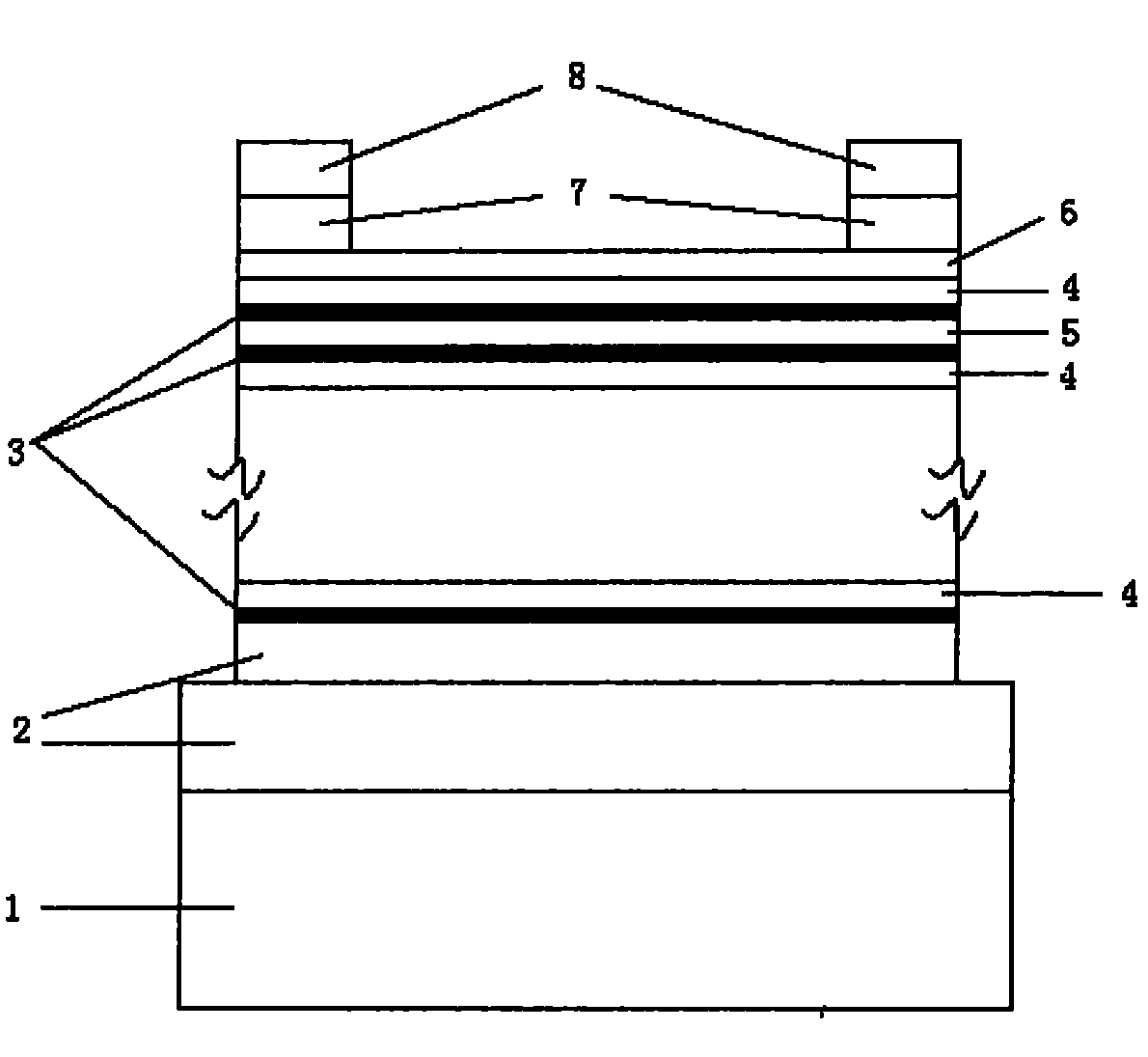
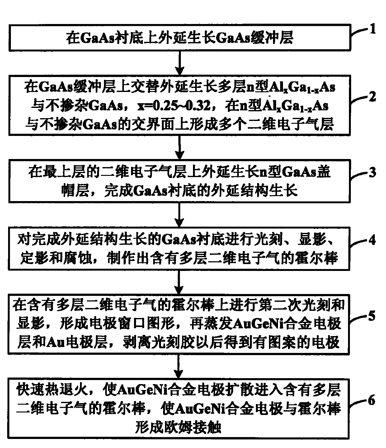
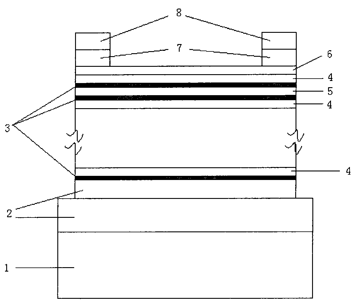
[0038] The present invention extends the concept of parallel connection from the plane direction of epitaxial wafers to the direction of epitaxial growth, that is, using epitaxial wafers containing multiple layers of two-dimensional electron gas, that is, growing on the substrate at one time during the growth process of epitaxial wafers For multi-layer two-dimensional electron gas, other device manufacturing processes except for the epitaxial growth process are compatible with single-layer two-dimensional electron gas epitaxial wafers. A three-dimensional quantized Hall series-parallel array can be fabricated by introducing parallel connections in the epitaxial growth direction.

[0039] like figure 1 as shown, figure 1...


PUM


Abstract

The invention discloses a quantum Hall resistance device containing multi-layer two-dimensional electron gas. The device consists of a GaAs buffer layer, a plurality of two-dimensional electron gas layers composed of n-type AlxGa1-xAs and undoped GaAs, an n-type GaAs nut cap layer epitaxially grown on a GaAs substrate from bottom to top in sequence, as well as an AuGeNi alloy electrode and an Au electrode deposited on the n-type GaAs nut cap layer in sequence, and x in the n-type AlxGa1-xAs is between 0.25 and 0.32. The invention also discloses a method for making the quantum Hall resistance device. The invention can reduce the scale of arrays and consumption of epitaxial wafer materials by times, lower the challenge in respect of the semi-conductor technique when making large-scale arrays and enhance the reliability of the arrays simultaneously.

Description

technical field [0001] The invention relates to the technical field of quantized Hall resistance, in particular to a quantized Hall resistance device containing a multi-layer two-dimensional electron gas and a manufacturing method thereof. Background technique [0002] Before 1980, countries in the world usually used the average value of the resistance of a set of standard resistance coils in metrology to maintain the resistance unit ohm. This kind of physical measurement reference realized by a special stable object has the following defects: once the physical reference is made, its characteristics will change slowly and slightly with the passage of time and temperature changes, and the quantity value they store There will also be changes. In addition, there is only one or one set of the highest level of physical measurement benchmarks in the world. Once accidental damage occurs, the original continuous preservation of the unit value will be interrupted. [0003] The Amer...

Claims


Application Information

Patent Timeline
Patent Type & Authority Patents(China)
IPC IPC(8): H01L43/08H01L43/06H01L43/10H01L43/14H01L43/12
Inventor 钟源钟青贺青张钟华李正坤鲁云峰赵建亭韩冰
Owner NAT INST OF METROLOGY CHINA
Why Eureka
Try Eureka