Method of forming electrochromic layer pattern, method of manufacturing electrochromic device using the same, and electrochromic device including electrochromic layer pattern

A technology of electrochromic devices and electrochromic layers, applied in instruments, nonlinear optics, optics, etc., can solve problems such as low productivity and reduced productivity

Inactive Publication Date: 2009-08-19
LG CHEM LTD
View PDF0 Cites 17 Cited by
  • Summary
  • Abstract
  • Description
  • Claims
  • Application Information

AI Technical Summary

Problems solved by technology

[0012] However, in the case of using a porous film to prepare the electrochromic layer 40, it is necessary to disperse nano-sized electrochromic particles in an organic solvent, apply it to a substrate in the form of a slurry, and then dry and sinter the solvent, This will result in lower productivity
In addition, the electrochromic layer 40 should have a thick thickness to obtain the desired coloring conditions, so there is a limit in thinning the ECD.
[0013] In addition, the method of patterning nano-sized holes in the electrochromic layer 40 shows low productivity because hole patterning requires a separate mask and also requires a number of additional steps such as mask alignment steps, photolithography steps, Etching step and cleaning step

Method used


Image

  • Method of forming electrochromic layer pattern, method of manufacturing electrochromic device using the same, and electrochromic device including electrochromic layer pattern
  • Method of forming electrochromic layer pattern, method of manufacturing electrochromic device using the same, and electrochromic device including electrochromic layer pattern
  • Method of forming electrochromic layer pattern, method of manufacturing electrochromic device using the same, and electrochromic device including electrochromic layer pattern

Examples


Embodiment Construction

[0046] Hereinafter, preferred embodiments of the present invention will be described in detail with reference to the accompanying drawings. Before the description, it should be understood that the terms in the specification and appended claims should not be construed as limited to the general and dictionary meanings, but on the basis of the principle of allowing the inventor to properly define the terms for the best interpretation, Explanations are made based on meanings and concepts related to the technical field of the present invention. Accordingly, the descriptions set forth herein are preferred embodiments for illustrative purposes only and are not intended to limit the scope of the invention, and it should therefore be understood that other modifications may be made thereto without departing from the spirit and scope of the invention. replace or improve.

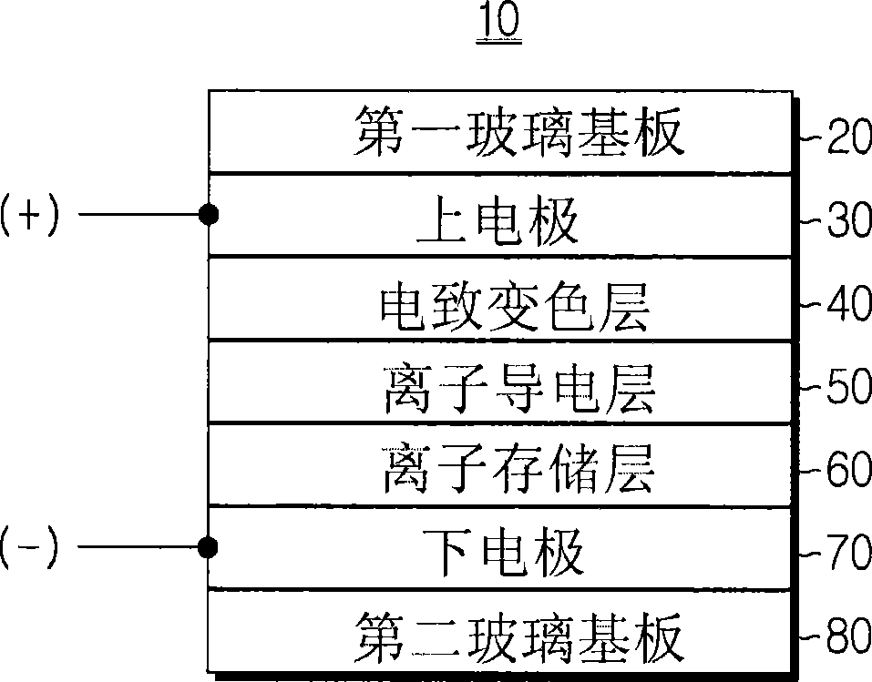
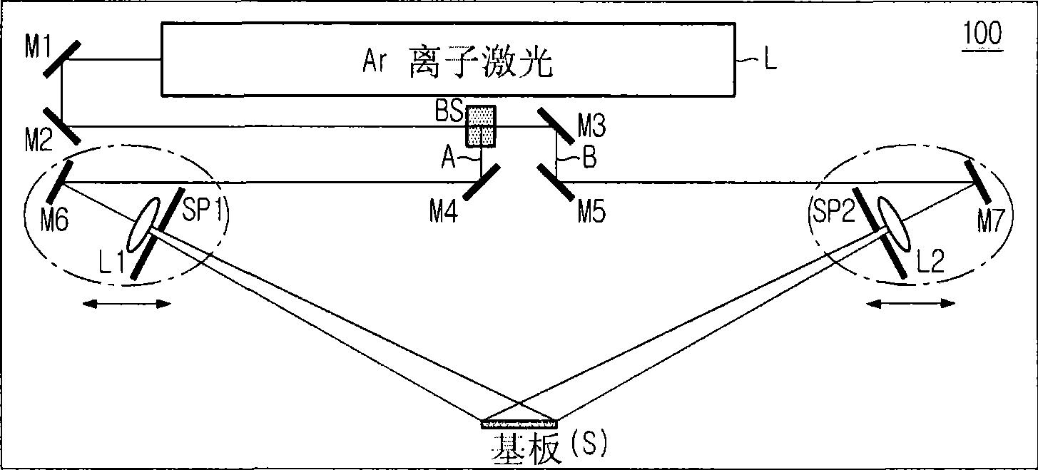
[0047] The method for forming the pattern of the electrochromic layer according to the present invention uses laser...


PUM


Abstract

A method for forming an electrochromic layer pattern includes forming a transparent electrode layer and a photoresist layer on a transparent substrate, forming a photoresist pattern by laser interference lithography, and depositing an electrochromic layer pattern on the transparent electrode through openings defined by the photoresist pattern by depositing an electrochromic layer on a front surface of the substrate and then lifting up the photoresist pattern. An insulation layer may be further formed between the transparent layer and the photoresist layer. Here, the electrochromic layer may be formed after an insulation layer pattern is formed using the photoresist pattern as an etching mask. In this case, the electrochromic layer pattern is formed in openings defined by the insulation layer pattern. As a result, a contact surface area between the electrochromic layer pattern and the ion conductive layer is increased to ensure a rapid response speed.

Description

technical field [0001] The present invention relates to a method for preparing an electrochromic device, and more particularly to a method for forming an electrochromic layer pattern of an electrochromic device, a method for preparing an electrochromic device using the above method, and an electrochromic device with an electrochromic layer pattern. Color changing device. Background technique [0002] An electrochromic device (ECD) is a color display device using an electrochromic material that is colored or decolorized by electrochemical oxidation or reduction depending on the direction in which an electric current is applied. The electrochromic operating methods are divided into cathodic and anodic operating methods. The cathodic electrochromic material forms color when reduced at an electrode composed of the negative pole, while the anodic coloring point to the color changing material either at the anode or at the positive pole. Additionally, if the direction of the curr...

Claims


Application Information

Patent Timeline
Patent Type & Authority Applications(China)
IPC IPC(8): G02F1/15
CPCG02F1/153G02F2001/164
Inventor 申铉雨张基硕朴真荣崔珉浩金台洙李守熙金载洪金芙敬
Owner LG CHEM LTD
Why Eureka
Try Eureka