Inductance coupling coil and plasma processing device adopting same

An inductively coupled coil and coil technology, applied in the field of microelectronics, can solve the problems affecting the uniformity of wafer processing/processing results, increase ion kinetic energy, increase coil inductance, etc., achieve good processing/processing results, uniform RF power distribution, improve The effect of coupling efficiency

Active Publication Date: 2009-08-26
BEIJING NAURA MICROELECTRONICS EQUIP CO LTD
View PDF1 Cites 31 Cited by
  • Summary
  • Abstract
  • Description
  • Claims
  • Application Information

AI Technical Summary

Problems solved by technology

However, increasing the coil length will cause an increase in the voltage across the coil, and an increase in the voltage across the coil will cause some of the RF power to couple into the plasma through capacitive coupling, that is, the capacitive coupling of the RF power from the coil to the plasma will increase as the voltage across the coil increases
However, capacitive coupling not only reduces the coupling efficiency of RF power, but also increases the kinetic energy of ions, making it difficult to precisely control the kinetic energy of ions, which in turn makes it difficult to precisely control process parameters such as sputtering rate and etching rate.
In addition, increasing the coil length will cause the coil inductance to also increase
However, if the inductance is too high, it will be difficult to achieve the conjugate matching of the coil, so that it is difficult to obtain the large-area, high-density and uniformly distributed plasma required for semiconductor processing, which will affect the uniformity of the processing / processing results of wafers and other workpieces

Method used


Image

  • Inductance coupling coil and plasma processing device adopting same
  • Inductance coupling coil and plasma processing device adopting same
  • Inductance coupling coil and plasma processing device adopting same

Examples


Embodiment Construction

[0043] In order to enable those skilled in the art to better understand the technical solution of the present invention, the present invention will be described in detail below in conjunction with the accompanying drawings.

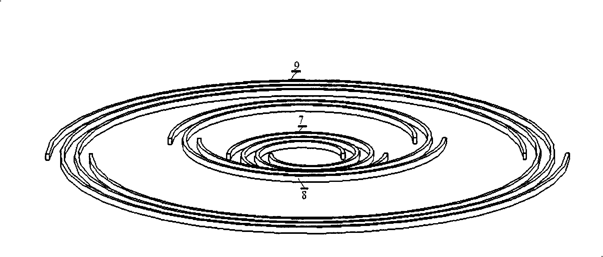
[0044] see image 3 The inductively coupled coil provided by the first embodiment of the present invention includes three sets of coil windings, namely, the innermost winding 7, the outermost winding 9, and the middle winding 8 between them. Wherein, each of the three sets of windings is a planar structure, and each set of windings includes two mutually nested helical coil branches.

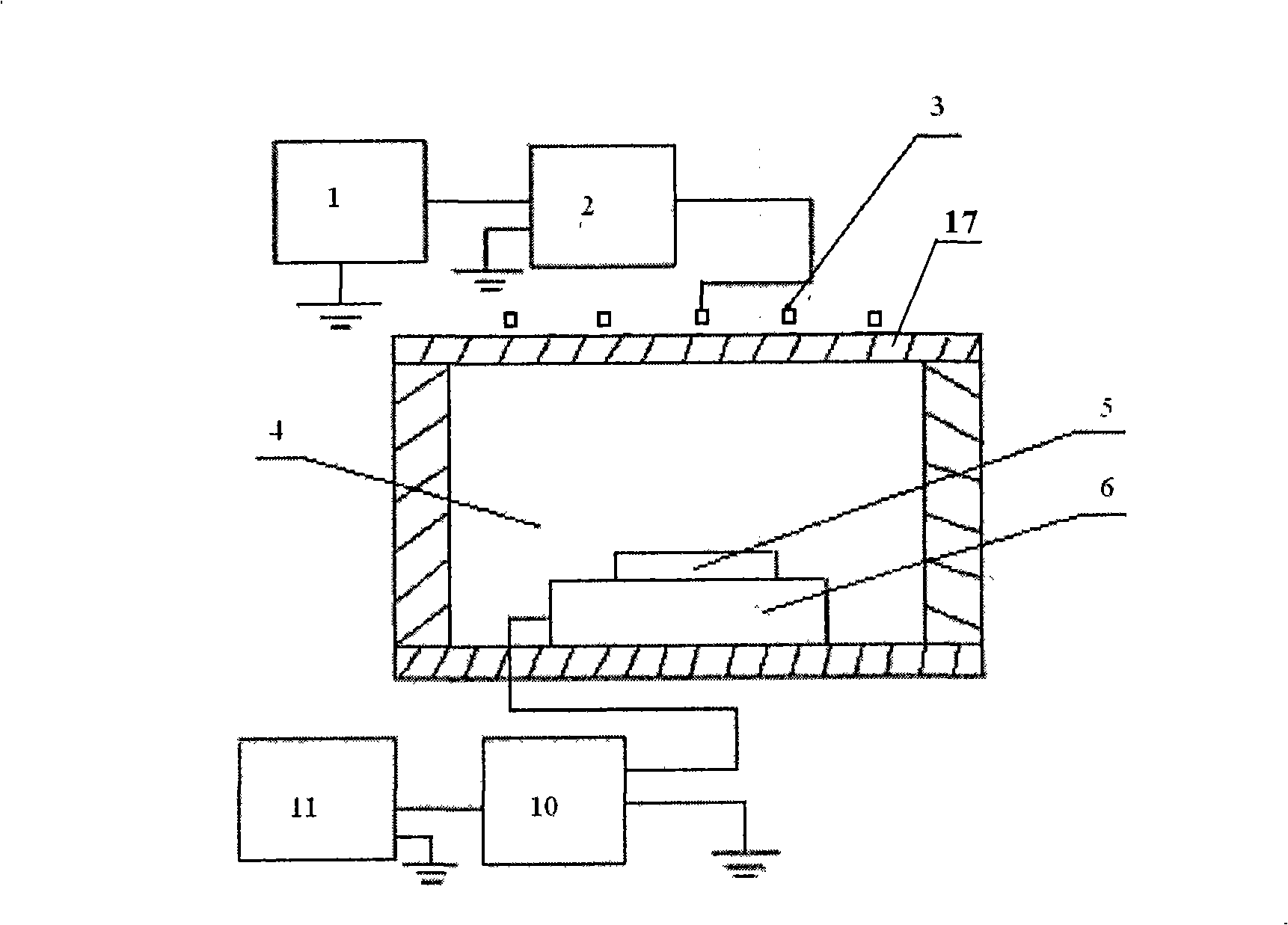
[0045] In practical applications, these three sets of coil windings are usually arranged on the dielectric window above the reaction chamber, but they are not located on the same plane, and the distance between the three sets of windings and the dielectric window can be set according to the actual process needs . Specifically, the distance between the upper surface of the ...


PUM

PropertyMeasurementUnit
sizeaaaaaaaaaa

Abstract

The invention discloses an inductance coupling coil, which comprises at least two groups of mutually nested coil windings with different diameters, wherein the upper surfaces of at least two groups of the coil windings in the coil windings are at planes with different heights for the convenience of obtaining plasmas which are distributed evenly. Besides, the invention also discloses a plasma processing device comprising a reaction chamber; a dielectric window is arranged on the upper part of the reaction chamber, and the inductance coupling coil is arranged above the dielectric window; and the inductance coupling coil is connected with a radio frequency power supply through a radio frequency matcher so as to obtain the plasmas distributed evenly in the reaction chamber. The inductance coupling coil and the plasma processing device can obtain the plasmas which are distributed evenly, and can obtain an excellent and even processing/handling result.

Description

technical field [0001] The invention relates to the technical field of microelectronics, in particular to an inductively coupled coil. In addition, the present invention also relates to a plasma processing device using the inductively coupled coil. Background technique [0002] With the rapid development of electronic technology, people have higher and higher requirements for the integration of integrated circuits, which requires companies that produce integrated circuits to continuously improve the processing / processing capabilities of semiconductor devices. At present, in the field of processing / processing of semiconductor devices, plasma etching technology and plasma deposition technology are often required, and these technologies are usually implemented by means of plasma processing devices such as plasma etching machines. [0003] Therefore, in the field of processing / handling of semiconductor devices, the working performance of a plasma processing device suitable for ...

Claims


Application Information

Patent Timeline
Patent Type & Authority Applications(China)
IPC IPC(8): H01F5/00H01F38/14H05H1/46H05H1/50H01L21/306
Inventor 韦刚李东三
Owner BEIJING NAURA MICROELECTRONICS EQUIP CO LTD
Why Eureka
Try Eureka