Semiconductor laser tube core sintering device and usage thereof

A sintering device and laser technology, which is applied in the direction of semiconductor lasers, lasers, laser components, etc., can solve the impact of laser device stability, reliability, life and yield, shift of light emitting direction, and uneven contact between chips and heat sinks and other problems, to achieve the effect of solving low luminous efficiency, reducing series resistance and thermal resistance, and good contact

Active Publication Date: 2009-08-26
吉光半导体科技有限公司
View PDF0 Cites 16 Cited by
  • Summary
  • Abstract
  • Description
  • Claims
  • Application Information

AI Technical Summary

Problems solved by technology

Manual operation is to manually pick up the die with tweezers, align it with the laser heat sink under a microscope, or use air tweezers to pick up the die and place it in the proper position of the heat sink, and then heat and sinter; during the sintering process, when the solder When melting, due to the existence of surface tension, if there is no proper top-down pressure on the chip, there will be problems such as the chip and the heat sink cannot be in uniform contact, and at the same time there will be problems such as shifting the direction of light emission, which will make the laser device stable and stable. Reliability, lifetime and yield are all severely impacted

Method used


Image

  • Semiconductor laser tube core sintering device and usage thereof

Examples


Embodiment Construction

[0015] The present invention is described in further detail below in conjunction with accompanying drawing:

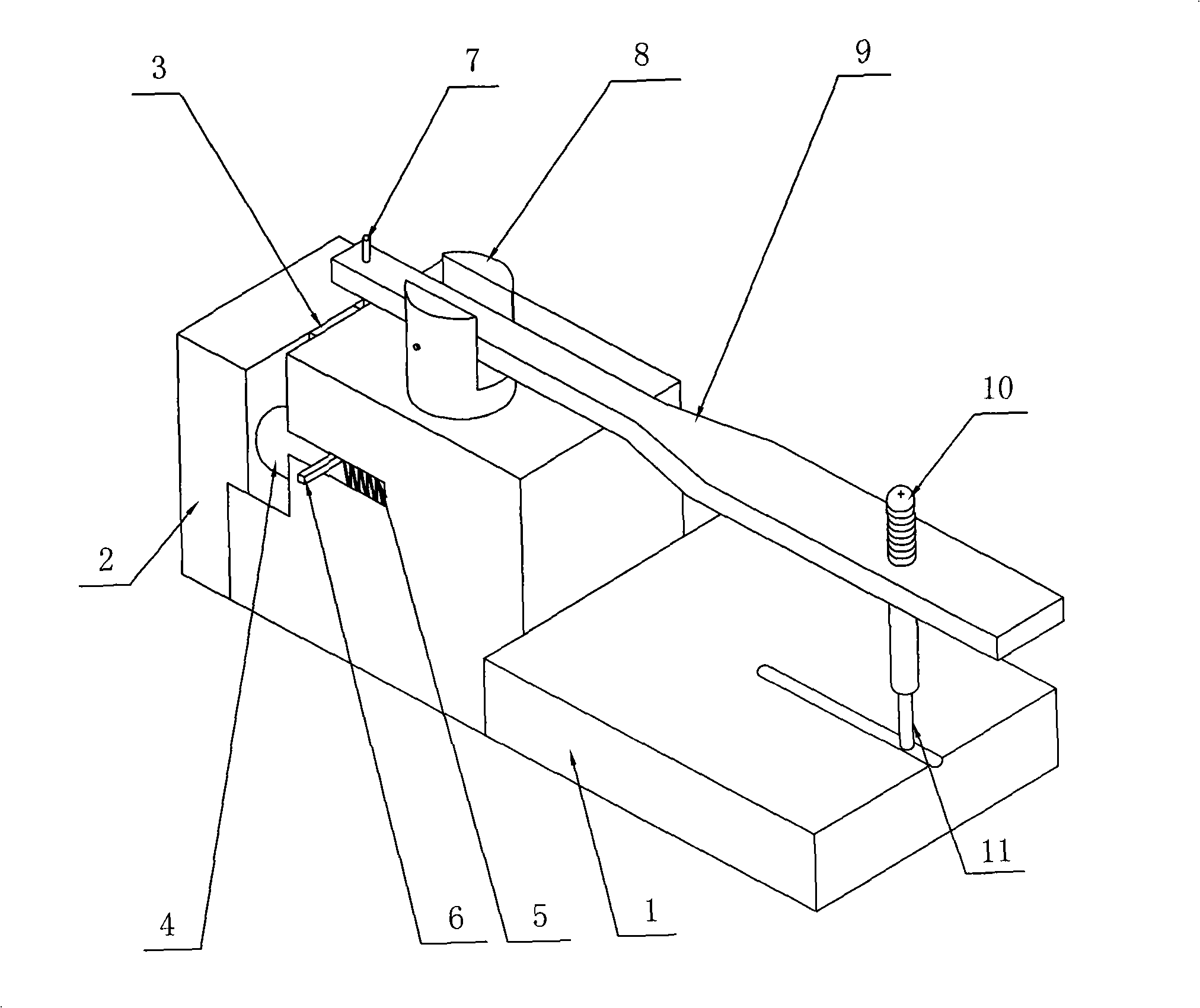
[0016] Such as figure 1 As shown, the semiconductor laser tube core sintering device of the present invention includes a bottom support 1, a front baffle plate 2, a heat sink 3, a pressure spring column 4, a spring 5, a puller 6, a pressure pin 7, a pillar 8, and a pressure rod 9 , the elastic pillar 10 and the sliding foot 11, the bottom support 1 and the front baffle 2 are fixedly connected by screws, the heat sink 3 is connected with the compression spring column 4 in contact, the spring 5 is elastically connected with the dial lever 6, and the pressure pin 7 is connected to the warp The pressure rod 9 is fixedly connected by screws, the pillar 8 is fixedly connected with the warping pressure rod 9 through chips, the warping pressure rod 9 is threadedly connected with the elastic pillar 10, the elastic pillar 10 is connected with the sliding foot 11 through spring c...


PUM

PropertyMeasurementUnit
diameteraaaaaaaaaa

Abstract

The invention provides a semiconductor laser tube core sintering device and usage thereof, belonging to the technical field of semiconductor optoelectronics; wherein the sintering device comprises a bottom supporting seat, a front baffle, heat sink, a pressure spring prop stay, a spring, a pushing plate, a pressing pin, a prop stay, a warp pressure lever, an elastic prop stay and a sliding foot; the heating and cooling processes of the sintering method are finished in a vacuum chamber and with the protection of nitrogen; firstly, the warp pressure lever is moved to a vacant position far away from the front baffle, then the warp pressure lever is moved under the observation of a microscope, the pressing pin is pressed on the chip exactly, then the device is placed in the vacuum chamber to be heated until the temperature increases to 170-200 DEG C, three minutes later the temperature of the device is decreased to 30-70 DEG C to finish the sintering of the tube core. The invention has the beneficial effects that the adoption of slide foot positioning sintering can simplify the exact positioning of the tube core sintering; the force on the chip applied by the pressing pin effectively reduces the serial resistance and thermal resistance of the tube core, thus resolving the problem of low lighting efficiency caused by tube core movement during melting; the process is simple and practical, the manufacture cost is low, and the productivity is high.

Description

technical field [0001] The invention belongs to the technical field of semiconductor optoelectronics, and relates to a semiconductor laser tube core sintering device and an application method thereof. Background technique [0002] At present, the die sintering of domestic semiconductor lasers generally adopts the method of manually placing the die under a microscope. Manual operation is to manually pick up the die with tweezers, align it with the laser heat sink under a microscope, or use air tweezers to pick up the die and place it in the proper position of the heat sink, and then heat and sinter; during the sintering process, when the solder When melting, due to the existence of surface tension, if there is no proper top-down pressure on the chip, there will be problems such as the chip and the heat sink cannot be in uniform contact, and at the same time there will be problems such as shifting the direction of light emission, which will make the laser device stable and sta...

Claims


Application Information

Patent Timeline
Patent Type & Authority Applications(China)
IPC IPC(8): H01S5/024H01S5/022
Inventor 刘云王立军刘长军宁永强秦丽
Owner 吉光半导体科技有限公司
Why Eureka
Try Eureka