Eureka AIR delivers breakthrough ideas for toughest innovation challenges, trusted by R&D personnel around the world.

Photolithographic system and method for measuring deviation between variable gap of photolithographic system and center of mask stage

A technology of lithography system and mask table, which is applied in the measurement field of lithography system and its variable slit and mask table center deviation, which can solve the problem of inaccurate description of relative deviation, low measurement accuracy, and increased measurement cost, etc. Problems, to achieve the effect of low cost, high measurement accuracy and easy operation

Active Publication Date: 2009-09-09
SHANGHAI MICRO ELECTRONICS EQUIP (GRP) CO LTD
View PDF1 Cites 2 Cited by
  • Summary
  • Abstract
  • Description
  • Claims
  • Application Information

AI Technical Summary

Problems solved by technology

However, this method requires the help of a third-party sensor, and can only measure the position of the variable slit boundary, and cannot accurately describe the relative deviation between the center of the mask table and the center of the variable slit in the lithography system
Not only increases the measurement cost, but also the measurement accuracy is not high

Method used


Image

  • Photolithographic system and method for measuring deviation between variable gap of photolithographic system and center of mask stage
  • Photolithographic system and method for measuring deviation between variable gap of photolithographic system and center of mask stage
  • Photolithographic system and method for measuring deviation between variable gap of photolithographic system and center of mask stage

Examples


Embodiment Construction

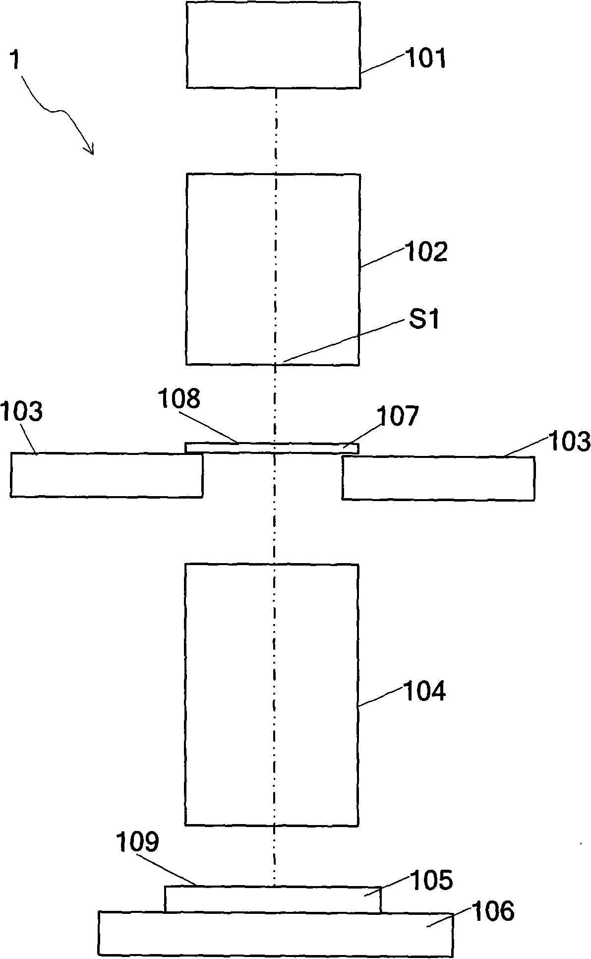
[0017] figure 1 A schematic diagram of a photolithography system according to a first embodiment of the present invention is shown. Such as figure 1 As shown, the lithography system 1 includes a light source 101 , an illumination system 102 with a variable slit S1 , a mask table 103 , a projection objective lens imaging system 104 , a wafer 105 and a table 106 for supporting and fixing the wafer. The photolithography system 1 also includes a reticle 107 . The reticle 107 is set on the mask table 103, and the reticle 107 includes a characteristic pattern 108 for identifying position deviation, and the characteristic pattern 108 forms an image 109 on the wafer 105 through the projection objective lens imaging system, by figure 1 It can be seen that the center of the reticle 107 coincides with the center of the mask table 103 .

[0018] In this embodiment, the light source 101 is a laser light source. The surface of the wafer has photoresist. In addition, in this embodiment,...


PUM


Abstract

The invention provides a photolithographic system and a method for measuring the deviation between a variable gap of the photolithographic system and a center of a mask stage. The photolithographic system comprises a light source, a lighting system with the variable gap, a mask plate, the mask stage for supporting and fixing the mask plate, a projection objective imaging system, a wafer and a worktable for supporting and fixing the wafer. The method for measuring the deviation between the variable gap of the photolithographic system and the center of the mask stage comprises the following steps: a feature pattern with a first center is designed on the mask plate and forms an image with a second center on the wafer by the projection objective imaging system; a first position where the first center is projected on the wafer is confirmed, a second position of the second center is confirmed; and the deviation between the variable gap and the center of the mask stage is calculated according to the first position and the second position. The system and the method directly utilize the feature pattern on the mask plate to calculate the deviation between the variable gap and the center of the mask stage, does not rely on a third-party sensor, is simple and convenient to operate and can reach extremely high measuring precision.

Description

technical field [0001] The present invention relates to a photolithography system and a measurement method, and in particular to a photolithography system and a method for measuring the center deviation between a variable slit and a mask table. Background technique [0002] Photolithography, or photolithography, has been widely used in integrated circuit manufacturing processes. This technology transfers the designed mask pattern to the photoresist through a photolithography device. The concepts of "mask" and "photoresist" are well known in the photolithography process: a mask is also called a photomask plate, which is a substrate with various functional patterns that are precisely positioned on a substrate such as a film, plastic or glass. A template used for selective exposure of the photoresist layer; photoresist is a colloidal liquid mixed with photosensitive compounds, matrix resins and organic solvents, and its chemical structure changes after being exposed to light o...

Claims


Application Information

Patent Timeline
Patent Type & Authority Applications(China)
IPC IPC(8): G03F7/20G03F1/14G01B11/03G03F1/44
Inventor 毛方林
Owner SHANGHAI MICRO ELECTRONICS EQUIP (GRP) CO LTD
Why Eureka
Eureka Blog
Learn More