Flat display

A flat-panel display, display panel technology, applied in static indicators, instruments, nonlinear optics, etc., can solve the problems that display panels and PCBs cannot use wireless communication, inconvenience, damage maintenance, etc.

Active Publication Date: 2009-09-16
KUSN INFOVISION OPTOELECTRONICS
View PDF0 Cites 11 Cited by
  • Summary
  • Abstract
  • Description
  • Claims
  • Application Information

AI Technical Summary

Problems solved by technology

[0007] With the structure of the above-mentioned traditional display, the communication between the display panel and the PCB cannot be in the form of wireless communication, and a wired connection method is required, such as FPC.
[0008] Further, the above-mentioned traditional flat-panel display with wired connection between the display panel and PCB determines that its manufacturing process is very complex and cumbersome, costly, and the wired connection between the display panel and PCB is easy to cause damage and inconvenient to repair.

Method used


Image

  • Flat display
  • Flat display
  • Flat display

Examples


Embodiment 1

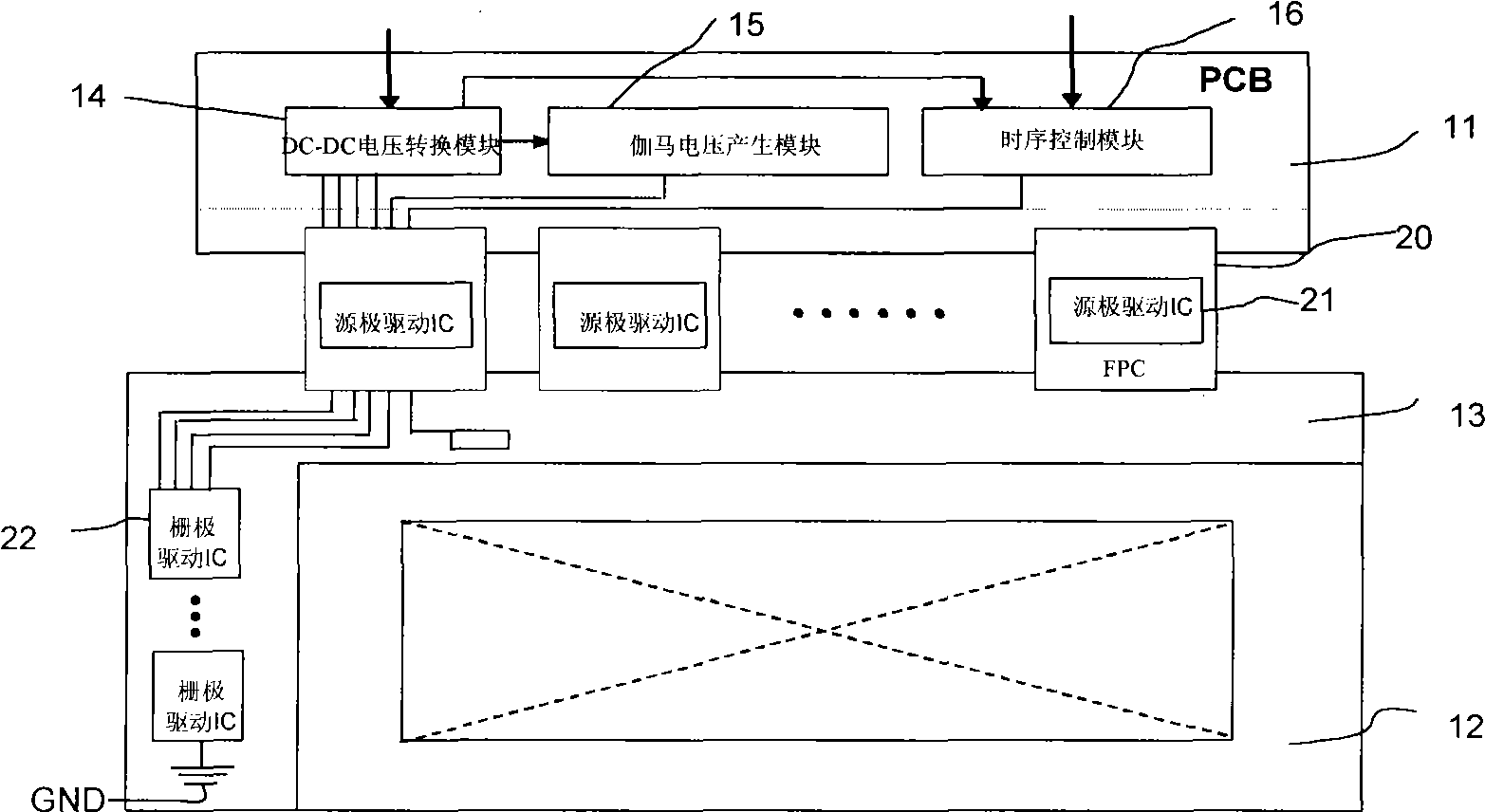
[0056] figure 2 It is a schematic diagram of the connection method between the PCB and the display panel of the first embodiment of the liquid crystal display of the present invention. Such as figure 2 As shown, the liquid crystal display includes: a display panel 210 , a PCB 220 and a wireless signal transmission device, and the wireless signal transmission device is used to realize wireless signal transmission between the PCB 220 and the display panel 210 .

[0057] Wherein, the display panel 210 includes two opposite substrates, that is, a first substrate 2130 and a second substrate 2140 . The gate driving IC 2112 is bonded on the side of the first substrate 2130 facing the second substrate 2140 through COG, and is located beside the display area 2135 , for example, on the left side. The source driver IC 2122 is COG bonded on the side of the first substrate 2130 facing the second substrate 2140 , and is located beside the display area 2135 , for example, above it. Ther...

Embodiment 2

[0093] In the second embodiment, the same part as the first embodiment will not be repeated, the difference is:

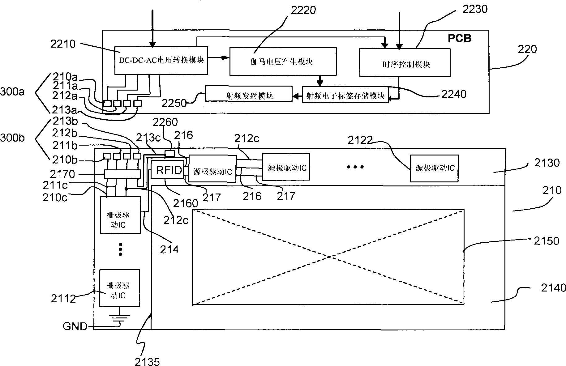
[0094] Such as Figure 8 As shown, the data signal transmission module includes a plurality of RFIDs arranged on the display panel, such as RFID 2160a, 2160b, 2160c, 2160d, 2160e, 2160f, and the plurality of RFIDs correspond to the gate drive IC and the source drive IC respectively. Conductive interconnection. Different source driver ICs use their corresponding RFIDs to directly receive signals, and different gate driver ICs use their corresponding RFIDs to directly receive signals. In this embodiment, the data signals corresponding to the corresponding gate driver ICs and source driver ICs are directly supplied through respective RFIDs, so that the stability and speed of data signal transmission are improved.

Embodiment 3

[0096] In the third embodiment, the same part as the first embodiment will not be repeated, the difference is:

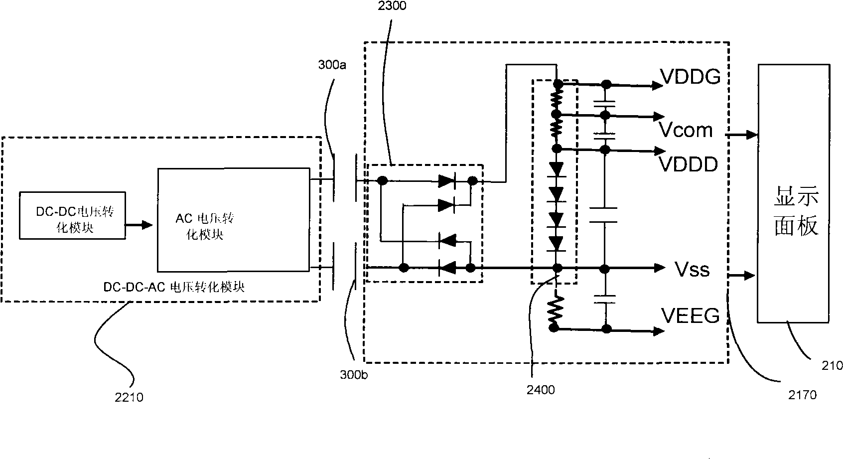
[0097] Such as Figure 9 As shown, the second capacitive coupling electrode 300b is respectively arranged beside the gate drive IC 2112, the source drive IC 2122, the common electrode connection terminal (not shown) and the RFID (not shown), the first capacitive coupling electrode 300a and the second The positions of the capacitive coupling electrodes 300b are in one-to-one correspondence. The liquid crystal display also includes an FPC810, and a gate drive IC side circuit board 820 connected to the PCB220 through the FPC810, a part of the first capacitive coupling electrodes 300a is located on the PCB, and another part of the first capacitive coupling electrodes 300a is located on the gate drive IC side circuit board . The power signal output by the DC-DC-AC voltage conversion module on the PCB is connected to the first capacitive coupling electrode 300a on the c...


PUM


Abstract

The invention discloses a flat display which includes a system circuit board and a display panel, also includes a wireless signal transmitting device for realizing transmission between the system circuit board and the display panel signal. The flat display sets a wireless signal transmitting device for transmitting wireless signal between he system circuit board and the display panel signal which can realize wireless communication between the display panel and the system circuit board, simplifies the flat display structure and corresponding manufacturing process and reduces cost.

Description

technical field [0001] The invention relates to the technical field of displays, in particular to a flat panel display. Background technique [0002] At present, an existing flat-panel display is to connect the system circuit board (PCB, printed circuit board) to the display panel through a flexible circuit board (FPC, flexible printedcable,), so that the PCB can provide the working power signal required by the display panel , and can control the display panel to display. [0003] A common liquid crystal display panel includes two opposite substrates, one of which has thin film transistors (TFT, thin film transistor) arranged in an array on the surface facing the other substrate, so it is called a TFT substrate. The gates of the plurality of rows of TFTs are connected to a gate driver IC, the sources of the plurality of rows of TFTs are connected to a source driver IC, and the drains of the TFTs are all connected to pixel electrodes on the TFT substrate. Usually, there are...

Claims


Application Information

Patent Timeline
Patent Type & Authority Applications(China)
IPC IPC(8): G09G3/20G09G3/36G02F1/13
Inventor 简廷宪崔宏青钟德镇
Owner KUSN INFOVISION OPTOELECTRONICS
Why Eureka
Try Eureka