Printed circuit board

A printed circuit board and pad technology, which is applied in the direction of printed circuit components and electrical components to assemble printed circuits, can solve problems such as short circuit of adjacent pads, overflow, and increased defective rate of printed circuit boards, and achieve good improvement. rate effect

Inactive Publication Date: 2009-09-16
INVENTEC PUDONG TECH CORPOARTION +1
View PDF0 Cites 6 Cited by
  • Summary
  • Abstract
  • Description
  • Claims
  • Application Information

AI Technical Summary

Problems solved by technology

In this way, if the pin spacing of the through-hole component to be installed in the printed circuit board is too small, the spacing of the pads corresponding to soldering each of the pins and arranged in the printed circuit board is also too small. When the pads on the printed circuit board tend to be arranged in a high density, during the wave soldering operation, it often occurs that the molten solder overflows and fuses between the adjacent two pads due to the small spacing during the wave soldering operation, resulting in adjacent solder pads. Pad short circuit problem
This kind of short circuit problem caused by solder overflow fusion has become the main factor for the increase in the defective rate of printed circuit boards

Method used


Image

  • Printed circuit board

Examples


Embodiment Construction

[0018] Embodiments of the present invention are described below through specific examples, and those skilled in the art can easily understand other advantages and effects of the present invention from the content disclosed in this specification.

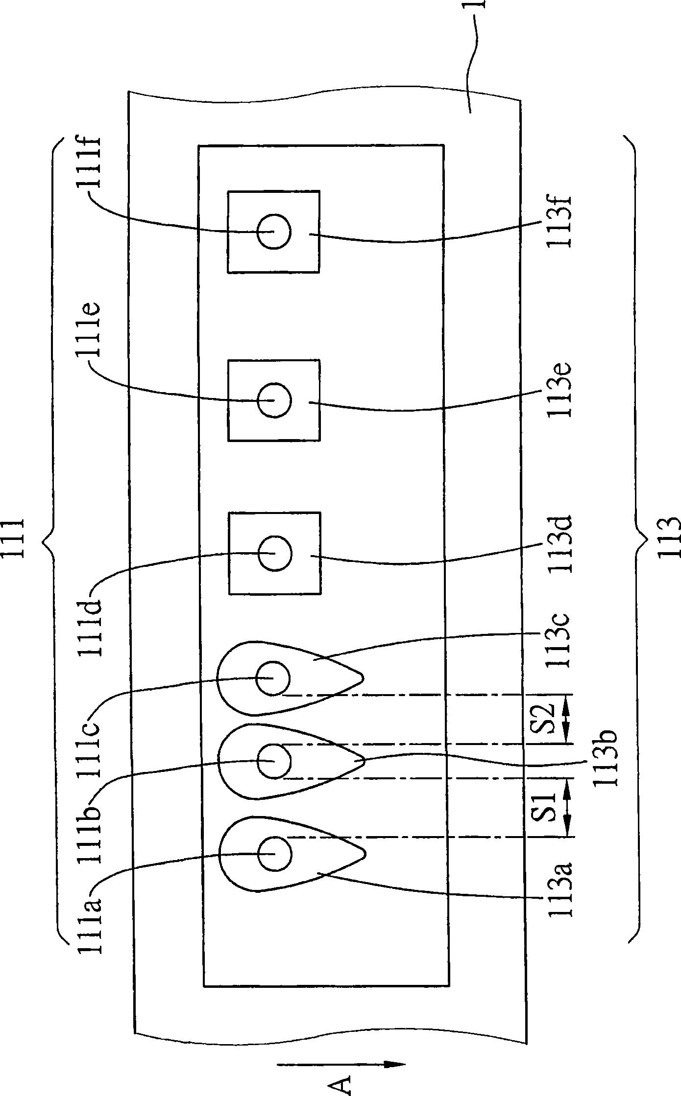
[0019] see figure 1 , showing a schematic diagram of the layout structure of the printed circuit board of the present invention. As shown in the figure, the printed circuit board 1 is provided with at least one soldering area 11 for corresponding connection with a through-hole component (Through-Hole Component; THC) having a plurality of pins (pins), and each of the pins There are at least two pins whose spacing is less than a specific distance, and the soldering area 11 has a plurality of through holes 111 that pass through the printed circuit board 1 and provide for correspondingly connecting each of the pins, and are arranged on the printed circuit board 1. 1 surface and disposed around the through hole 111 for soldering a plural...


PUM


Abstract

A printed circuit board comprises at least two adjacent through holes penetrating through the board and two bonding pads. Each bonding pad encloses the through hole and is arranged on the surface of the printed circuit board and used for welding a perforation type subassembly, wherein each bonding pad takes the shape with a tapered end so that soldering tin overflows along the direction of the tapered end in the welding process, thus further preventing the soldering tin from overflowing to an adjacent bonding pad and then causing short circuit.

Description

technical field [0001] The present invention relates to a printed circuit board, and more particularly, to a printed circuit board that prevents adjacent pads from being short-circuited. Background technique [0002] Although most of the printed circuit board designs currently use the hybrid assembly technology of double-sided patches, surface mount technology (Surface Mount Technology; SMT) has become the development trend of printed circuit board design technology, but many components such as inductance coils and high-power components Components such as power modules and power modules still cannot use the above-mentioned surface mount technology due to reasons such as heat dissipation, component materials, and reliability. Instead, through-holes are opened in the printed circuit board and assembled by perforation. Therefore, the above-mentioned components are also called through-hole components ( Through Hole Component; THC), this type of perforated component still occupie...

Claims


Application Information

Patent Timeline
Patent Type & Authority Applications(China)
IPC IPC(8): H05K1/02H05K3/34
Inventor 张兰范文纲
Owner INVENTEC PUDONG TECH CORPOARTION
Why Eureka
Try Eureka