6H-SiC substrate reversed polarity AlGaInP LED chip

A reverse polarity, substrate technology, applied in electrical components, circuits, semiconductor devices, etc., can solve problems such as incompatibility with high current, high output power, etc., to improve high temperature characteristics, improve product reliability, and high thermal conductivity. Effect

Inactive Publication Date: 2009-09-23
Shandong Huaguang Optoelectronics Co. Ltd.
View PDF0 Cites 10 Cited by
  • Summary
  • Abstract
  • Description
  • Claims
  • Application Information

AI Technical Summary

Problems solved by technology

[0005] The present invention aims at the problem that the existing AlGaInP quaternary light-emitting diode chip adopts GaAs substrate and is not suitable for working conditions of high current and high output power, and provides a 6H-SiC substrate reverse polarity AlGaInP LED chip with high current and high output power and Its manufacturing method, and a manufacturing process of the LED chip is provided at the same time

Method used


Image

  • 6H-SiC substrate reversed polarity AlGaInP LED chip
  • 6H-SiC substrate reversed polarity AlGaInP LED chip
  • 6H-SiC substrate reversed polarity AlGaInP LED chip

Examples


Embodiment 1

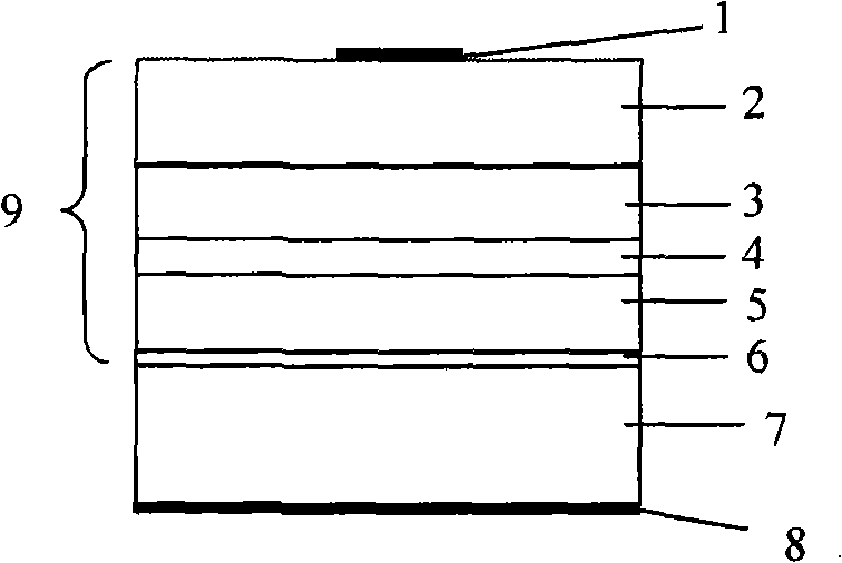
[0026] The 6H-SiC substrate reverse polarity AlGaInP LED chip of this embodiment is based on conductive 6H-SiC, and its chip structure is as follows figure 2 As shown, the epitaxial layer 9 is also included, but the epitaxial layer 9 is an N-type AlGaInP layer 5, a light-emitting layer 4, a P-type AlGaInP layer 3, a P-type GaP layer 2, and a metal reflection and bonding layer 10 (including An adhesive layer and a metal mirror), and an N-type electrode 8 is arranged on the N-type AlGaInP layer 5 (the top surface of the epitaxial layer 9). The epitaxial layer 9 is grown on the conductive 6H-SiC substrate 11 , and the P-type electrode 1 is arranged on the bottom surface of the conductive 6H-SiC substrate 11 . It can be seen that the present invention is based on the 6H-SiC material whose thermal conductivity is 10 times higher than the GaAs material, and transfers the LED light-emitting layer from the GaAs substrate to the 6H-SiC substrate, which is different from the existing A...

Embodiment 2

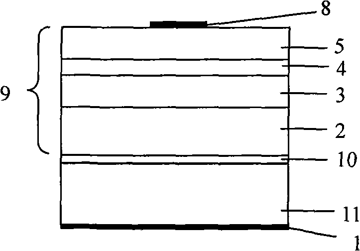
[0034] The 6H-SiC substrate reverse polarity AlGaInP LED chip of this embodiment is based on insulating 6H-SiC, such as image 3 As shown, the insulating 6H-SiC substrate 12 is used to replace the conductive 6H-SiC substrate 11 of Example 1, and the P-type electrode 1 is fabricated on the metal reflective and bonding layer 10, and the rest of the structure is the same as that of Example 1 with the conductive 6H-SiC substrate 11. The reverse polarity AlGaInP quaternary LED chip based on SiC is the same.

[0035] The manufacturing process steps of the reverse polarity AlGaInP LED chip based on the insulating 6H-SiC of the present embodiment are as follows:

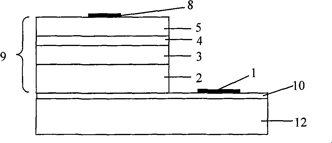
[0036] 1. If Figure 4 As shown, the LED epitaxial structure is also grown on the GaAs substrate 7 according to the conventional epitaxial growth, and the N-type AlGaInP layer 5, the light-emitting layer 4, the P-type AlGaInP layer 3 and the P-type GaP layer 2 are epitaxially grown in sequence from bottom to top to form an ...


PUM


Abstract

The invention discloses a 6H-SiC substrate reversed polarity AlGaInP LED chip and a manufacturing process thereof. The reversed polarity AlGaInP LED chip comprises a substrate and an epitaxial layer on the substrate, wherein a 6H-SiC material is used as the substrate; and the epitaxial layer sequentially comprises an N-type AlGaInP layer, a light emitting layer, a P-type AlGaInP layer, a P-type GaP layer and a metal reflecting and bonding layer from top to bottom; the N-type AlGaInP layer is provided with an N-type electrode; and the bottom surface of the 6H-SiC substrate or the metal reflecting and bonding layer is provided with a P-type electrode. The manufacturing process comprises the steps that the surface of the 6H-SiC substrate is provided with the metal reflecting and bonding layer in a vapor deposition mode; the epitaxial layer and the substrate are bonded together; then a selective corrosion method is used for corroding and peeling off an original CaAs underlay; and the electrode formed by the processes of vapor deposition, corrosion, and the like is manufactured into a pipe core. The 6H-SiC substrate reversed polarity AlGaInP LED chip uses the 6H-SiC substrate material with high heat conductivity as the substrate and transfers an LED light emitting layer onto the 6H-SiC substrate so as to improve the high-temperature characteristics of products and improve the reliability of the products.

Description

technical field [0001] The invention relates to a structure of a quaternary AlGaInP light-emitting diode (LED) chip and a manufacturing method thereof, belonging to the technical field of semiconductor optoelectronic processing. Background technique [0002] High-brightness AlGaInP quaternary LEDs have the advantages of long life, good stability, energy saving and environmental protection, and are widely used in indoor and outdoor display screens, urban lighting, traffic lights, automotive lights, liquid crystal display backlights and other fields. [0003] The existing conventional AlGaInP quaternary LED chips use GaAs substrates, and the chip structure is as follows figure 1 As shown, it includes an epitaxial layer 9 and a GaAs substrate 7. The top surface of the epitaxial layer 9 is provided with a P-type electrode 1, and the bottom surface of the GaAs substrate 7 is provided with an N-type electrode 8. The epitaxial layer 9 is a P-type GaP layer from top to bottom. 2. A...

Claims


Application Information

Patent Timeline
Patent Type & Authority Applications(China)
IPC IPC(8): H01L33/00
Inventor 徐现刚夏伟苏建
Owner Shandong Huaguang Optoelectronics Co. Ltd.
Why Eureka
Try Eureka