Explosion-proof module structure for power components, particularly power semiconductor components, and production thereof

A power module and power device technology, which is applied in semiconductor devices, semiconductor/solid-state device components, electric solid-state devices, etc., can solve problems such as high conduction voltage, overheating of power semiconductor devices, and damage of power semiconductor devices

Inactive Publication Date: 2011-05-25
SIEMENS AG
View PDF1 Cites 0 Cited by
  • Summary
  • Abstract
  • Description
  • Claims
  • Application Information

AI Technical Summary

Problems solved by technology

Although this limits the voltage at which the arc is driven, the other power semiconductors overheat in this case, since these power semiconductors have a high conduction voltage when controlled via the collector potential
This causes all parallel connected power semiconductors to be destroyed until the current is completely interrupted

Method used


Image

  • Explosion-proof module structure for power components, particularly power semiconductor components, and production thereof
  • Explosion-proof module structure for power components, particularly power semiconductor components, and production thereof
  • Explosion-proof module structure for power components, particularly power semiconductor components, and production thereof

Examples


Embodiment Construction

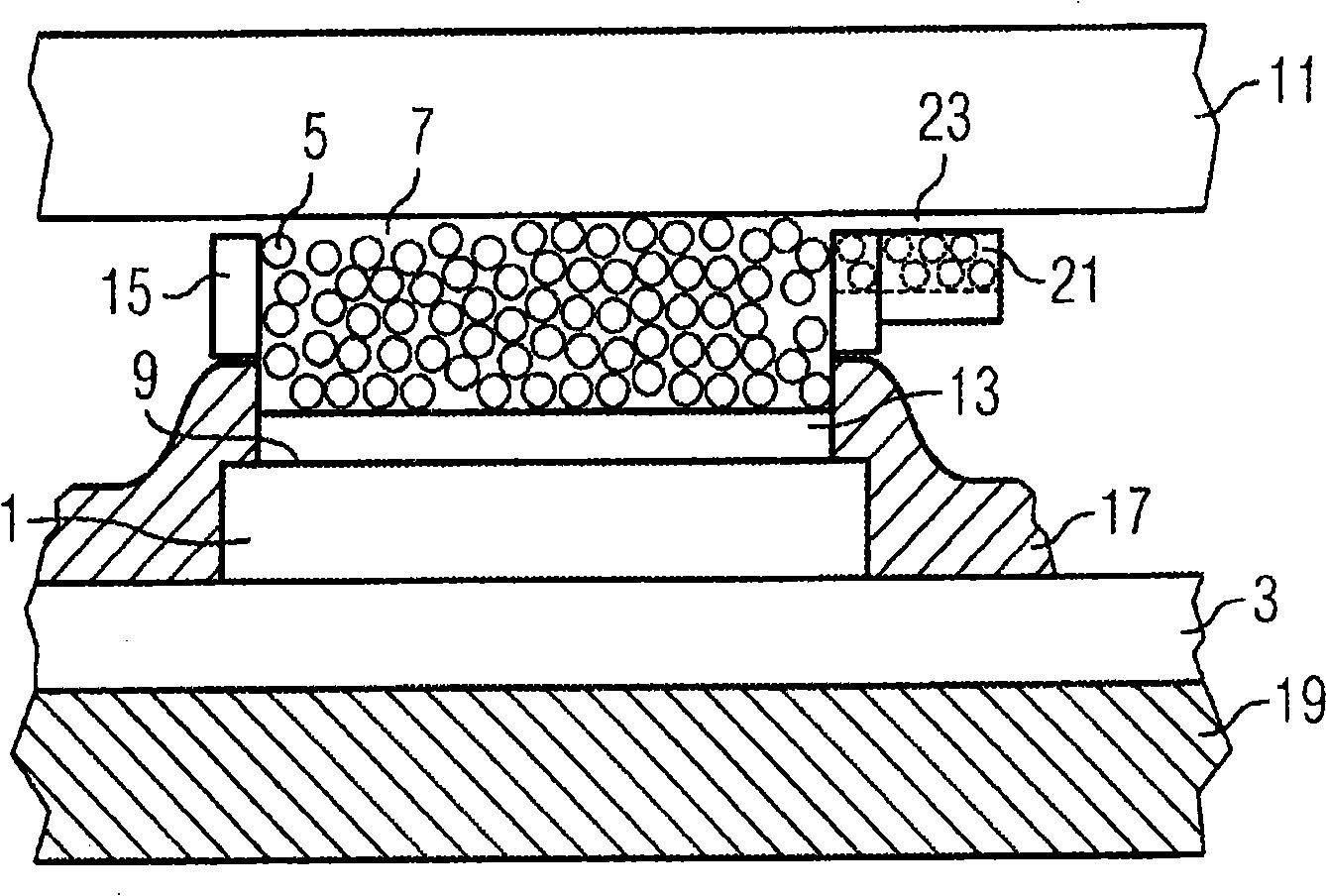
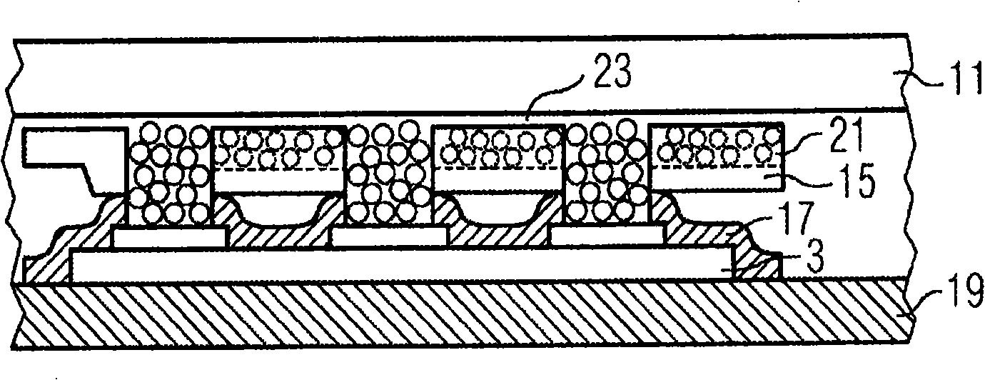
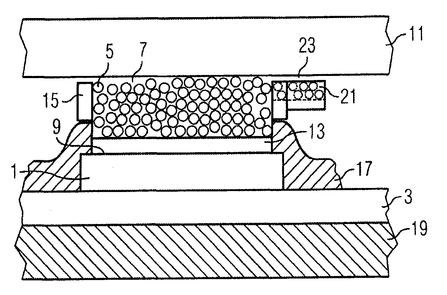
[0029] figure 1 The first embodiment of the power module according to the present invention is shown. According to the explosion-proof module structure, the explosion pressure is leaked by the filling consisting of conductive particles 5 (for example, metal balls with a diameter of 0.5 mm to 2 mm) and a channel 23 for pressure reduction, where the channel 23 for pressure reduction is along Box 15 is generated. According to this embodiment, a power device is realized, in particular, an electronic power semiconductor device 1 is realized. The electronic power semiconductor device 1 has a first load current generated on the bottom side of the power semiconductor device 1. Electrical contact. Furthermore, by means of the electrical contact surface 9, a second electrical contact for the load current is produced on the upper side of the power semiconductor component 1. The power semiconductor device 1 is arranged on a substrate 19. The first electrical contact on the side facing t...


PUM


Abstract

The invention relates to power modules, particularly power modules comprising at least one electric power component, especially a power electronic semiconductor component (1). An electrical contact for a load current is created on a lower surface and an upper surface of said power semiconductor component (1). In order to reduce an explosion pressure and accept power when the power electronic semiconductor component (1) is overloaded, a hollow space (7) that is filled with at least one electrically conducting particle (5) is formed on an electrical contact surface (9) of the electrical contact. In case of a short circuit, an arc is initially generated above the semiconductor element thickness of the power semiconductor component (1), whereupon the filling in the hollow space (7) takes overcurrent conduction. Preferably, the filling in the hollow space (7) is embodied as a plurality of spherical electrically conducting particles (5). The explosion pressure can escape into the interstices in the filling in case of a short circuit. Furthermore, metal vapors are cooled and are condensed. A duct extending from the hollow space (7) out of the hollow space (7) can additionally be createdin order to reduce the explosion pressure, thus preventing power components from demolishing the surroundings thereof during an electrical overload. The invention makes it possible to improve a thyristor, for example.

Description

Technical field [0001] The invention relates to all power modules having at least one electric power device, especially an electronic power semiconductor device. Power devices are all electrical devices or electronic devices that can be used for high current or high power. Then, an electronic power semiconductor device exemplified for all possible power devices is explained. Background technique [0002] In a conventional manner, power modules, in particular modules with power semiconductor components, are contacted by means of bonding. Power semiconductor modules especially have electronic power semiconductor components. Such electronic power semiconductor devices are used to generate controllable energy for large consumers, and can connect large load currents. Power semiconductors must be protected from overvoltage, excessive voltage rise speed, short circuit, excessive current rise speed, and thermal overload. Especially when a short circuit occurs in the consumer, the ele...

Claims


Application Information

Patent Timeline
Patent Type & Authority Patents(China)
IPC IPC(8): H01L23/18
CPCH01L2924/01013H01L2924/01082H01L2924/01002H01L2924/01033H01L23/48H01L2924/01079H01L25/072H01L2924/01047H01L23/62H01L2924/13055H01L23/18H01L23/043H01L24/72H01L2924/01029H01L2924/01045H01L2924/01006H01L2924/19043H01L2924/01044H01L2924/01058H01L2924/1301H01L2924/13033H01L2924/1305H01L2924/00
Inventor H·施沃兹鲍尔
Owner SIEMENS AG
Why Eureka
Try Eureka