Supercharge Your Innovation With Domain-Expert AI Agents!

Method for manufacturing TFT-LCD array substrate and color film substrate

A manufacturing method and an array substrate technology, which are applied in the photolithographic process of the patterned surface, semiconductor/solid-state device manufacturing, instruments, etc., can solve the problems of many production processes, long time, and reduced TFT-LCD production efficiency, etc., and achieve improved Production efficiency, the effect of guaranteeing product characteristics

Active Publication Date: 2009-09-30
K TRONICS (SUZHOU) TECH CO LTD +1
View PDF0 Cites 25 Cited by
  • Summary
  • Abstract
  • Description
  • Claims
  • Application Information

AI Technical Summary

Problems solved by technology

[0004] At present, in the prior art TFT-LCD production process based on the MVA mode, the formation of pixel electrodes and array bumps on the array substrate is formed in two processes such as photolithography, etching, stripping and cleaning. The formation of common electrodes and color filter bumps is also formed in two processes of photolithography, etching, stripping and cleaning. There are many production processes and a long time, which greatly reduces the production efficiency of TFT-LCD.

Method used


Image

  • Method for manufacturing TFT-LCD array substrate and color film substrate
  • Method for manufacturing TFT-LCD array substrate and color film substrate
  • Method for manufacturing TFT-LCD array substrate and color film substrate

Examples


Embodiment Construction

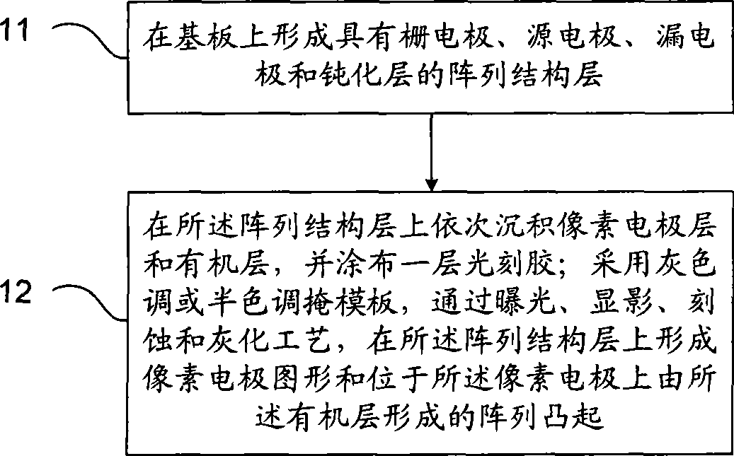
[0065] figure 1 It is a flow chart of the manufacturing method of the TFT-LCD array substrate of the present invention, specifically:

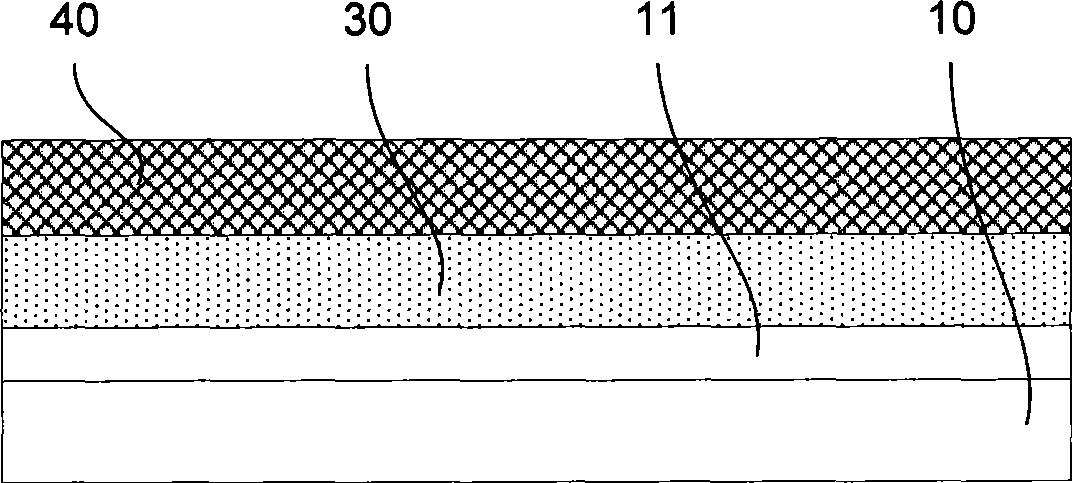
[0066] Step 11, forming an array structure layer having a gate electrode, a source electrode, a drain electrode and a passivation layer on the substrate;

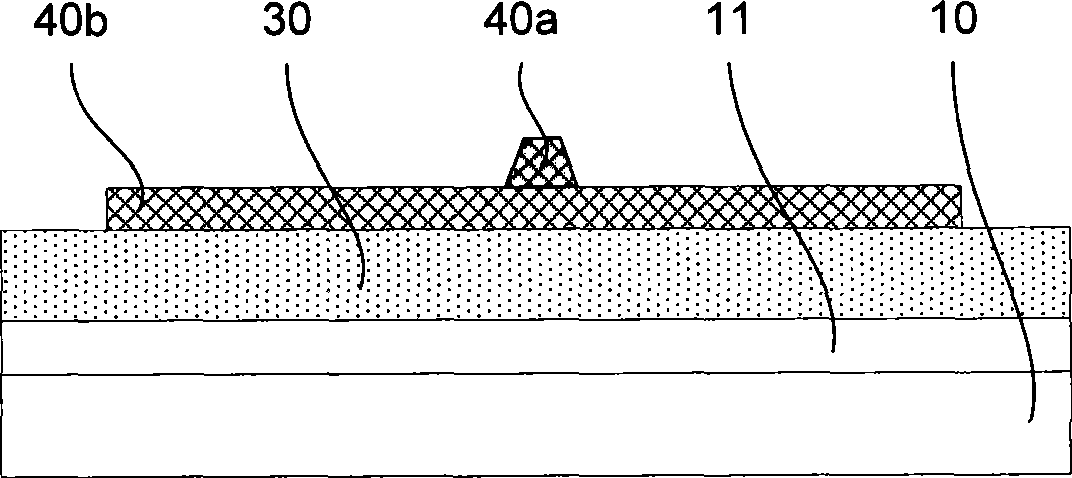
[0067] Step 12, sequentially depositing a pixel electrode layer and an organic layer on the array structure layer, and coating a layer of photoresist; using a gray-tone or half-tone mask, through exposure, development, etching and ashing processes, the A pixel electrode pattern and an array protrusion formed by the organic layer on the pixel electrode are formed on the array structure layer.

[0068] The invention provides a method for manufacturing a TFT-LCD array substrate based on the MVA mode. By using a gray tone or half tone mask, the two patterning processes for forming pixel electrodes and array protrusions in the prior art are integrated into one patterning process. , while impr...


PUM


Abstract

The invention relates to a method for manufacturing a TFT-LCD array substrate and a color film substrate. The method for manufacturing the array substrate comprises the steps: an array structural layer comprising gate electrodes, source electrodes, drain electrodes and deactivation layers is formed on the substrate, a pixel electrode layer and an organic layer are deposited on the array structural layer in sequence, a layer of photoresist is coated on the array structural layer, and a pixel electrode pattern and an array gray lug boss which is formed by the organic layer and arranged on the pixel electrode are formed on the array structural layer by adopting a grey tone or shadow tone mask plate and by the processes of exposing, developing, etching and ashing. The method adopts the grey tone or shadow tone mask plate and integrates the two pattern-forming processes for forming the pixel electrode and the array lug boss into one pattern-forming process, thereby increasing the production efficiency and ensuring the product characteristics of the TFT-LCD array substrate.

Description

technical field [0001] The invention relates to a method for manufacturing a liquid crystal display device, in particular to a method for manufacturing a TFT-LCD array substrate and a color filter substrate based on an MVA mode. Background technique [0002] Thin Film Transistor Liquid Crystal Display (TFT-LCD for short) has the characteristics of small size, low power consumption, no radiation, and relatively low manufacturing cost, and occupies a dominant position in the current flat panel display device market. With the gradual expansion of the application field of TFT-LCD, an MVA-based TFT-LCD suitable for large-screen display is proposed in the prior art. The Multi-Domain Vertical Alignment (MVA) mode is a display device with the advantages of high contrast, fast response and wide viewing angle, which can make the large-screen display device have better picture quality. [0003] Figure 19 It is a cross-sectional view of a TFT-LCD based on MVA mode in the prior art, ta...

Claims


Application Information

Patent Timeline
Patent Type & Authority Applications(China)
IPC IPC(8): H01L21/84G02F1/1362G02F1/1335G03F7/00G03F7/42
Inventor 明星周伟峰郭建
Owner K TRONICS (SUZHOU) TECH CO LTD
Features
  • R&D
  • Intellectual Property
  • Life Sciences
  • Materials
  • Tech Scout
  • Unparalleled Data Quality
  • Higher Quality Content
  • 60% Fewer Hallucinations
Learn More