Manufacturing method of semiconductor device

A manufacturing method, a semiconductor technology, applied in the direction of semiconductor/solid-state device manufacturing, electrical components, circuits, etc., can solve problems such as rising manufacturing costs, gate defects, poor electrical properties of components, etc., to reduce process costs and save the number of masks Effect

Active Publication Date: 2011-03-16
VANGUARD INTERNATIONAL SEMICONDUCTOR CORPORATION
View PDF0 Cites 0 Cited by
  • Summary
  • Abstract
  • Description
  • Claims
  • Application Information

AI Technical Summary

Problems solved by technology

In the known semiconductor process, after forming the gate, for components with different thicknesses of the gate insulating layer, a full-scale etching method can be used to remove the remaining gate insulating layer, but due to the The thickness difference of the remaining gate insulation layer is still too large, which will cause unwanted substrate loss or gate defects, resulting in poor electrical performance and reduced reliability of the component
However, the method of increasing the number of masks to remove the remaining gate insulating layer located in different component regions will increase the manufacturing cost

Method used


Image

  • Manufacturing method of semiconductor device
  • Manufacturing method of semiconductor device
  • Manufacturing method of semiconductor device

Examples


Embodiment Construction

[0033] Use the following Figure 1 to Figure 5 , to describe the method for manufacturing a semiconductor device according to the embodiment of the present invention in more detail. In various embodiments of the present invention, the same symbols represent the same or similar components.

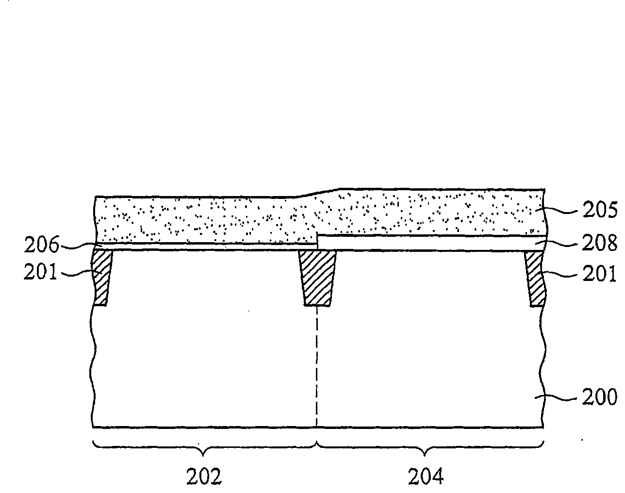
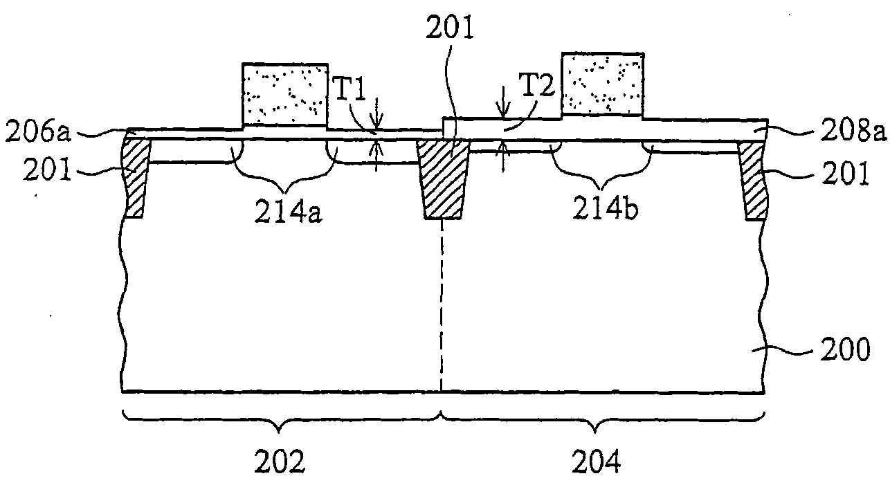
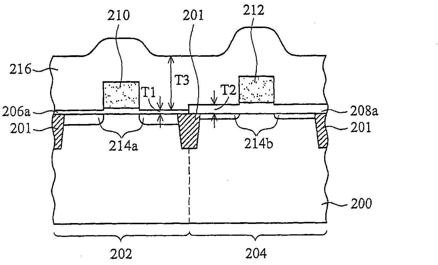
[0034] Please refer to figure 1 , which shows a process cross-sectional view of a semiconductor device according to an embodiment of the present invention. First, a substrate 200 is provided. In a preferred embodiment of the present invention, the substrate 200 may be a silicon substrate. In other embodiments, silicon germanium (SiGe), bulk semiconductor (bulk semiconductor), strained semiconductor (strained semiconductor), compound semiconductor (compound semiconductor), silicon on insulating layer (silicon insulator, SOI), or Other common semiconductor substrates. The substrate 200 can be implanted with P-type or N-type impurities to change its conductivity type according to design n...


PUM


Abstract

The invention provides a manufacturing method of a semiconductor device. The method includes the steps: respectively forming a first gate insulation layer and a second gate insulation layer on a base plate; roundly forming a gate layer; removing part of the gate layer, the first gate insulation layer and part of the second gate insulation layer to form a first gate, a first residual gate insulation layer, a second gate and a second residual gate insulation layer, wherein the first residual gate insulation layer which is not covered by the first gate is provided with a first thickness, the second residual gate insulation which is not covered by the second gate is provided with a second thickness, and the ratio of the first thickness and the second thickness is between 1:10 and 1:20; and respectively forming a pair of first gap walls and a pair of second gap walls on the side walls of the first gate and the second gate. The invention can avoid the problems of poor electric property or lowered reliability of an assembly, save the amount of masks used by the process and lower the process cost.

Description

technical field [0001] The present invention relates to a manufacturing method of a semiconductor device, in particular to a process for integrating a semiconductor device including a plurality of components with different gate insulating layer thicknesses. Background technique [0002] With the continuous advancement of semiconductor process shrink technology, and the stringent requirements for size and function of portable and consumer products, System on a Chip (SoC) has become the mainstream trend of integrated circuit design in the electronics industry. In one SoC, logic components, memory components, analog components and various input / output (I / O) interfaces are provided, so one chip has complete system operation functions. For example, a liquid crystal display chip needs to be driven by a high voltage metal oxide semiconductor transistor (HVMOS) driven by a high voltage (such as 30V or 40V), and driven by a low or medium voltage (such as 2.5V or 5V). ) logic circuit...

Claims


Application Information

Patent Timeline
Patent Type & Authority Patents(China)
IPC IPC(8): H01L21/82
Inventor 林治平陈世明杨晓莹刘文贤胡博胜
Owner VANGUARD INTERNATIONAL SEMICONDUCTOR CORPORATION
Why Eureka
Try Eureka