Method for preparing masking microstructure

A microstructure and microgroove technology, applied in microstructure technology, microstructure devices, manufacturing microstructure devices, etc., can solve the problems of relying on etching equipment, difficult processing, complex preparation process, etc., to achieve optimization and microgroove. Passivation process, eliminating process parameter adjustment, avoiding the effect of dependence

Inactive Publication Date: 2009-10-21
PEKING UNIV
View PDF0 Cites 22 Cited by
  • Summary
  • Abstract
  • Description
  • Claims
  • Application Information

AI Technical Summary

Problems solved by technology

[0005] The existing preparation process is complicated, the processing is difficult, and the yield is low
Usually only circular cross-sections can be obtained, even if the cross-sectional shape can be controlled, it still depends on sophisticated etching equipment and complex process parameters
In addition, if the process parameters are changed, it may also lead to poor flatness of the inner wall of the flow channel

Method used


Image

  • Method for preparing masking microstructure
  • Method for preparing masking microstructure
  • Method for preparing masking microstructure

Examples


Embodiment Construction

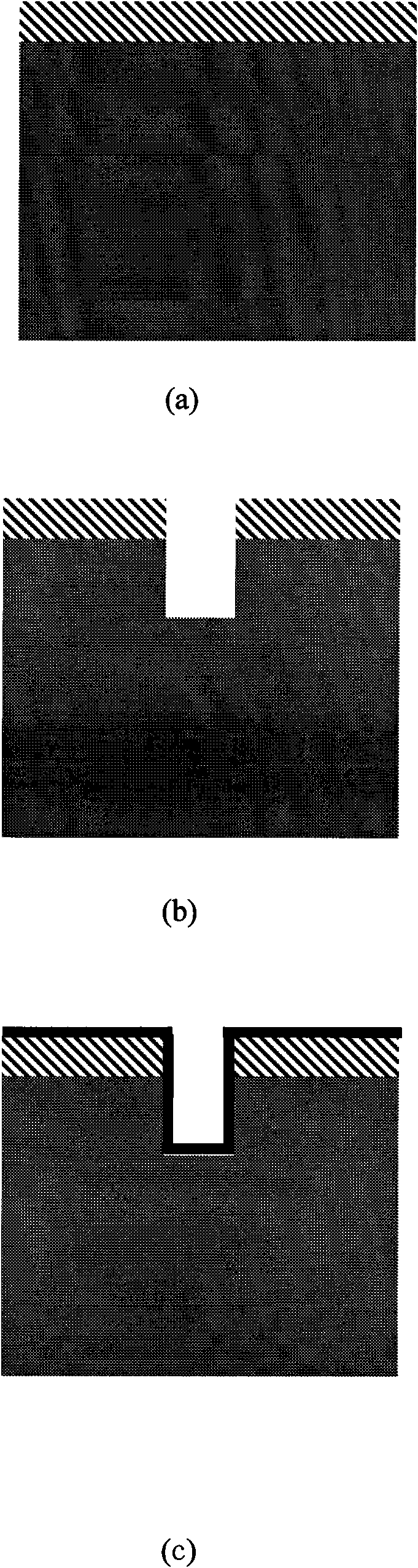
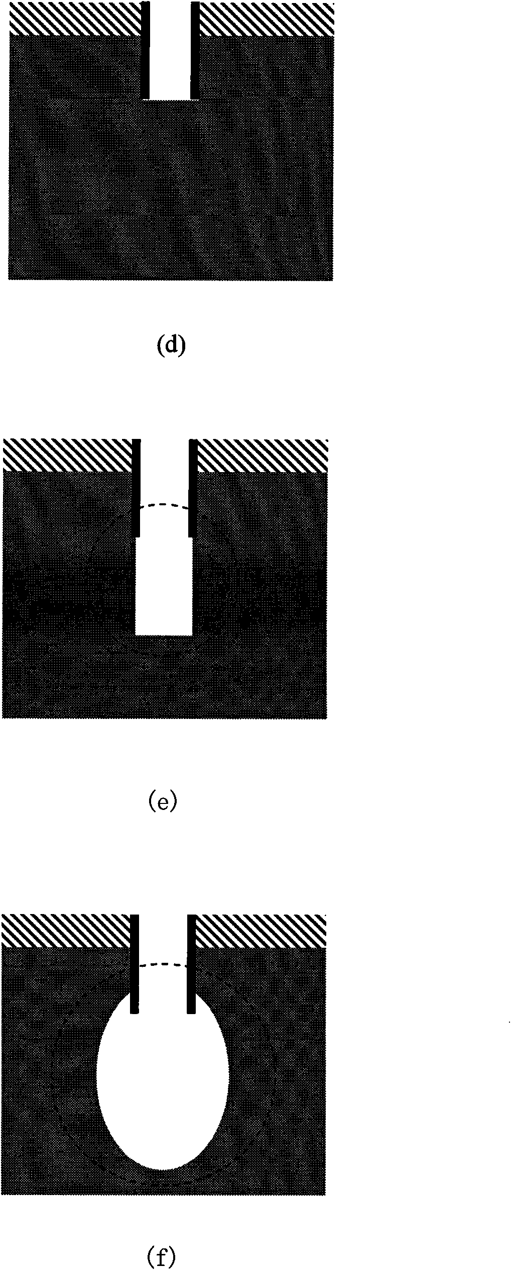
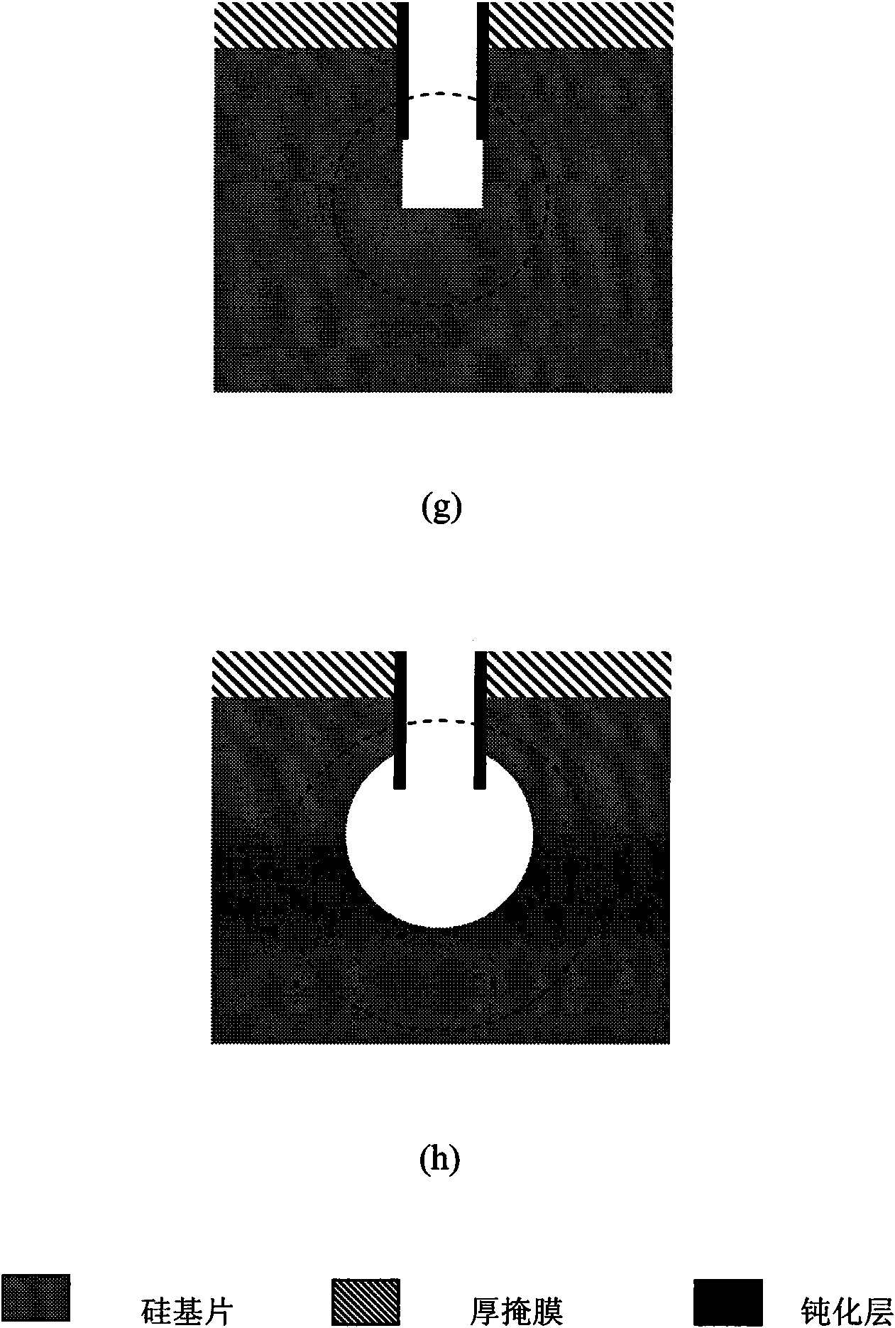
[0028] Below in conjunction with accompanying drawing and specific embodiment the present invention is described in further detail:

[0029] Taking the preparation process of microchannel as an example, the preparation steps are as follows: figure 1 shown, including:

[0030] 1. Thick silicon oxide mask preparation:

[0031] Thick silicon oxide is grown by thermal oxidation, with a thickness of 1 μm, such as figure 1 as shown in (a);

[0032] 2. Etching microgrooves:

[0033] Photolithography, and then etch the plane pattern of the microgroove, the opening width of the microgroove is 3 μm, and the silicon is deeply etched 8 μm, such as figure 1 as shown in (b);

[0034] 3. Surface passivation:

[0035] LPCVD deposited silicon dioxide with a thickness of 250nm, such as figure 1 as shown in (c);

[0036] 4. Etching the bottom mask of the microgroove

[0037] RIE anisotropically etches the silicon dioxide at the bottom of the microgroove, such as figure 1 as shown in (d...


PUM

PropertyMeasurementUnit
thicknessaaaaaaaaaa
widthaaaaaaaaaa
sizeaaaaaaaaaa

Abstract

The invention discloses a method for preparing a masking microstructure, and belongs to the technical field of microelectronic mechanical systems. The method comprises the following steps: preparing a silicon dioxide mask of which thickness is 1 to 2mu m on the surface of a silicon substrate, patterning the mask, and deeply etching silicon to form a micro-groove or micro-opening structure; carrying out surface passivation for the micro-groove or micro-opening structure; removing a bottom passivation layer of the micro-groove or micro-opening structure by etching, and pre-etching the bottom of the micro-groove or micro-opening structure; next, continuously carrying out isotropic etching to form a microstructure; then, removing the mask on the surface of the silicon substrate and the passivation layer on the side wall of the micro-groove or micro-opening structure; and backfilling the microstructure to form the masking microstructure. The method uses the thick mask to well protect the surface of the silicon substrate so as to avoid the phenomenon of pinholes and under etching. Because the isotropic etching of the masking microstructure is carried out after the pre-etching, the section shape of the masking microstructure can be controlled, the complex process parameter adjustment is avoided, and the dependency on precision etching equipment is also avoided.

Description

technical field [0001] The invention relates to a micro-electro-mechanical system (MEMS) technology of a silicon process, in particular to a method for preparing a masked microstructure. Background technique [0002] Microfluidic system is an important branch of the MEMS field, which is widely used in the fields of microelectronics, micromechanics and bioengineering. Its design idea is to realize complex fluid control operations by constructing microfluidic channels. In the existing processing technology, the method of combining side wall passivation and plasma etching can be used to process the micro flow channel or micro chamber structure covered under the surface of the substrate. The processing flow of masking microchannels is roughly divided into: surface silicon oxide, silicon nitride mask growth, microgroove etching, sidewall passivation, and microchannel etching. The advantage of this type of preparation process is that after the flow channel is completed, the surfa...

Claims


Application Information

Patent Timeline
Patent Type & Authority Applications(China)
IPC IPC(8): B81C1/00
Inventor 张大成李婷刘鹏王玮罗葵田大宇李静王颖
Owner PEKING UNIV
Why Eureka
Try Eureka