Supercharge Your Innovation With Domain-Expert AI Agents!

Method and device for acquiring optimal parameters of photoetching machine

A technology of optimal parameters and lithography machine, applied in the direction of photolithography exposure device, micro-lithography exposure equipment, etc., can solve the problems of increasing the complexity of lithography machine and the impact of the service life of silicon wafers, and achieves a wide range of applications, Strong versatility and saving raw materials

Inactive Publication Date: 2009-10-21
PEKING UNIV FOUNDER GRP CO LTD +1
View PDF6 Cites 8 Cited by
  • Summary
  • Abstract
  • Description
  • Claims
  • Application Information

AI Technical Summary

Problems solved by technology

In this way, multiple trial engravings are required, which increases the complexity of lithography machine debugging. Although the silicon wafers after trial engraving can be reused, the service life of the silicon wafers is also affected.

Method used


Image

  • Method and device for acquiring optimal parameters of photoetching machine
  • Method and device for acquiring optimal parameters of photoetching machine
  • Method and device for acquiring optimal parameters of photoetching machine

Examples


Embodiment Construction
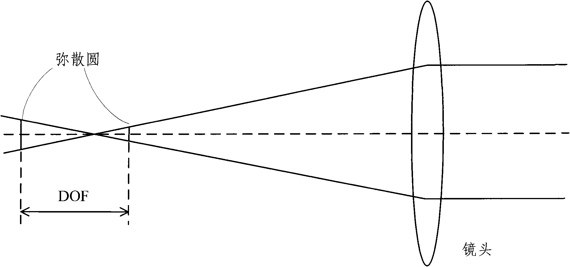
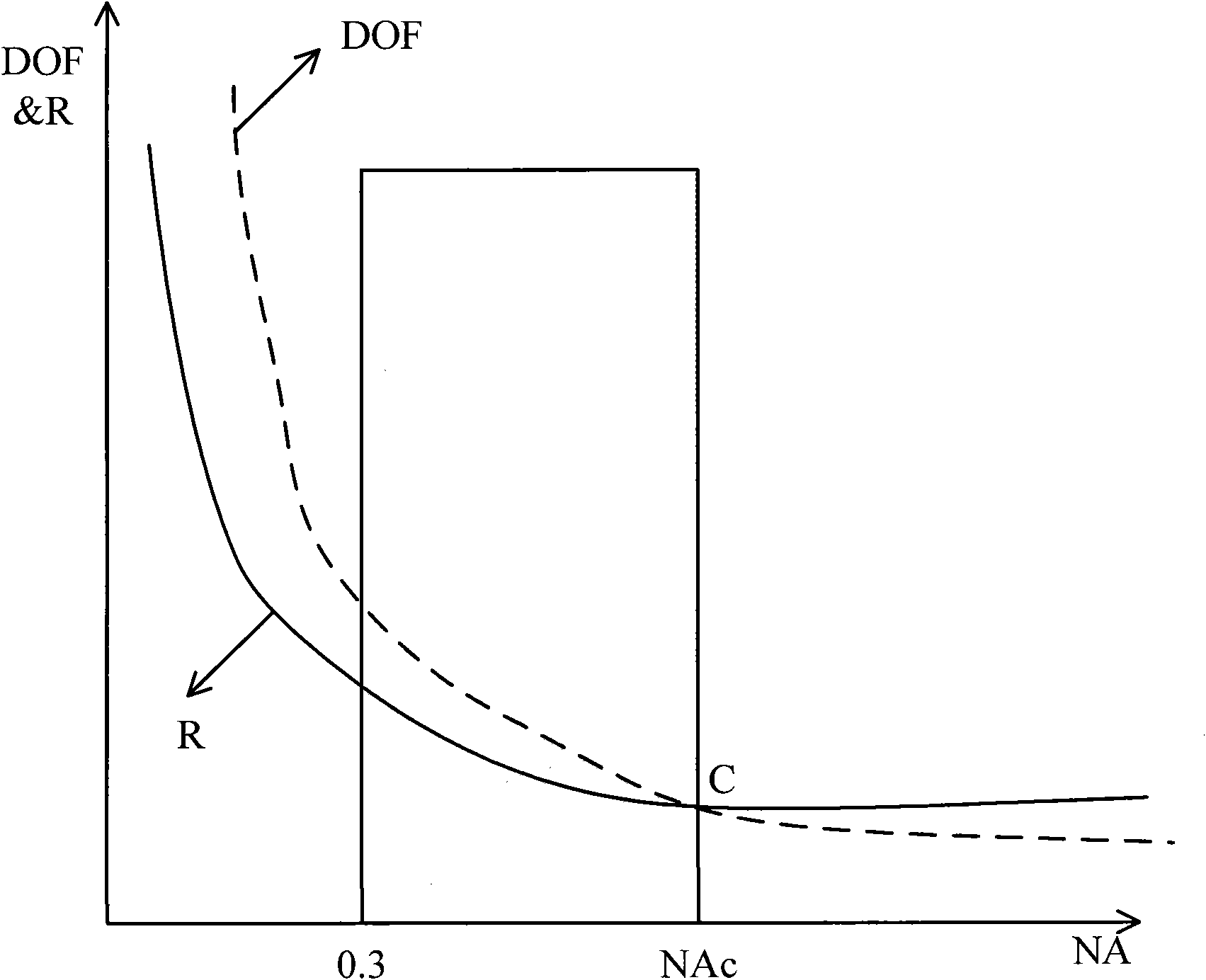
[0036] The basic idea of ​​the present invention is: based on the NA value, gradually calculate the resolution and depth of field corresponding to each NA value from the initial NA value to the truncated numerical aperture NAc value, and select and output the best one according to the required resolution. A set of parameters is given to the user; furthermore, according to the output parameters, the adjustment effect of the lithography machine can be simulated, which can reduce the trial marking of silicon wafers and save costs.

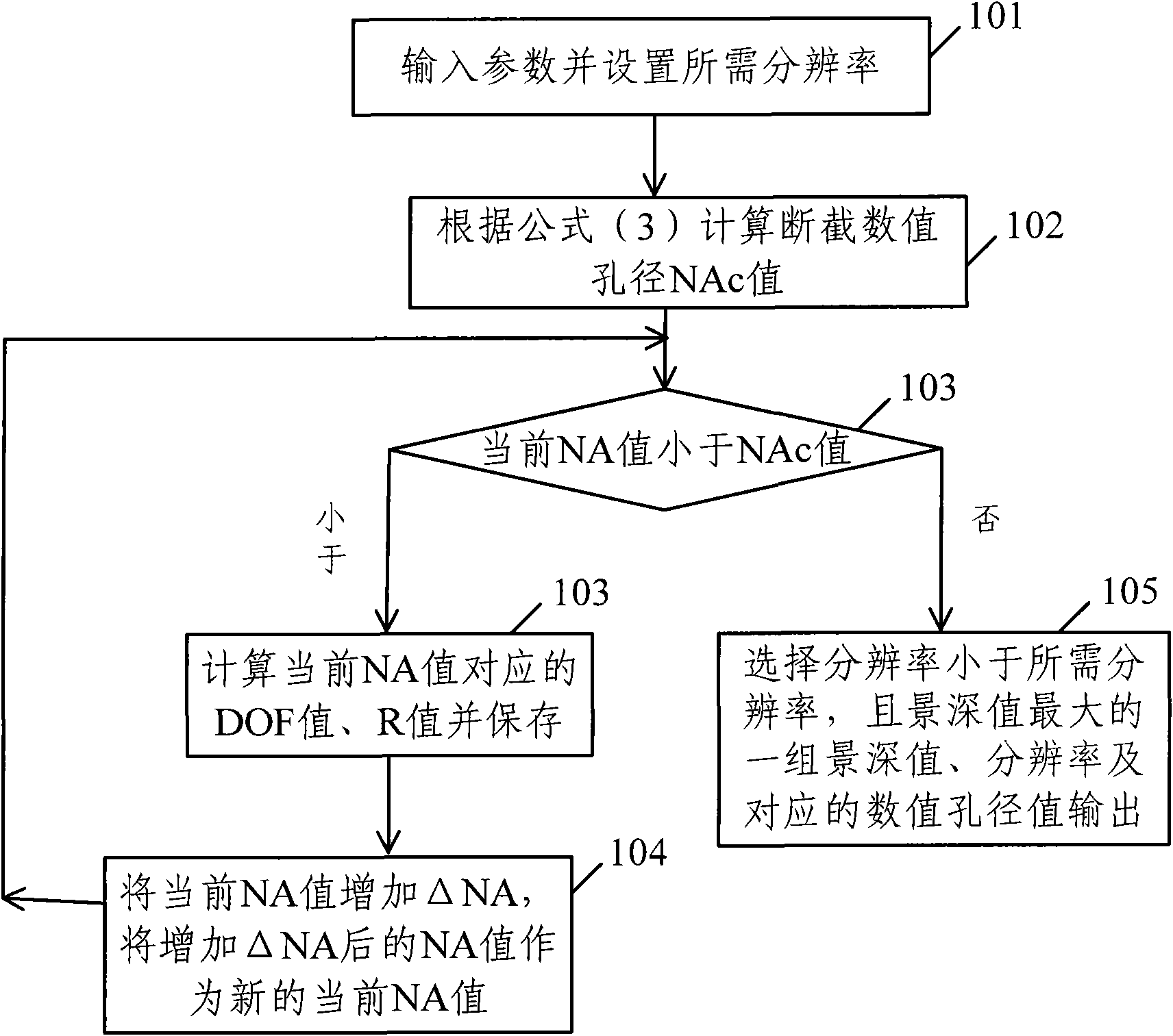
[0037] Below in conjunction with accompanying drawing, concrete method of the present invention is realized and further described, as image 3 As shown, the method includes:

[0038] Step 101, input parameters and set required resolution.

[0039] Here, the input parameters include the wavelength λ of the exposure light source, the photoresist constant K 1 , photoresist constant K 2 , initial NA value and NA value increasing step size ΔNA.

[0040...


PUM


Abstract

The invention discloses a method for acquiring optimal parameters of a photoetching machine. The method is used for setting the required resolution and comprises the following steps: inputting parameters and calculating cut off numerical aperture value; judging whether the current numerical aperture value is less than the cut off numerical aperture value, if so, calculating and saving depth of focus value and the resolution which correspond to the current numerical aperture value; increasing the numerical aperture value, using the increased step length of numerical aperture as new current numerical aperture value, and recalculating the numerical aperture value; and otherwise, selecting and outputting the a set of depth of focus values of which the resolution is less than the required resolution and the depth of focus value is largest, the resolution and the numerical aperture value corresponding to the depth of focus value and the resolution. The invention also discloses a device for acquiring optimal parameters of a photoetching machine, which selects and outputs an optimal set of depth of focus values, the resolution and the corresponding numerical aperture value. The method improves the machine debugging efficiency and prolongs the service life of the silicon chips.

Description

technical field [0001] The invention relates to a semiconductor photolithography process, in particular to a method and a device for obtaining optimal parameters of a photolithography machine. Background technique [0002] Lithography machine is one of the core technologies of semiconductors, mainly used in the photolithography process of ultra-small line width graphics of semiconductors. Usually, before the mass production of the lithography machine, the parameters of the lithography machine need to be debugged to ensure the use effect of the lithography machine. In the process of lithography machine debugging, there are two important parameters that need to be handled carefully, namely resolution (Resolution) and depth of field (DOF, Depth Of Focus). Depth of field involves the concept of the circle of confusion. The so-called circle of confusion means that light begins to gather and diffuse before and after the focal point of the lens, and the image gradually becomes blu...

Claims


Application Information

Patent Timeline
Patent Type & Authority Applications(China)
IPC IPC(8): G03F7/20
Inventor 骆国泉林大野刘鹏飞
Owner PEKING UNIV FOUNDER GRP CO LTD
Features
  • R&D
  • Intellectual Property
  • Life Sciences
  • Materials
  • Tech Scout
  • Unparalleled Data Quality
  • Higher Quality Content
  • 60% Fewer Hallucinations
Learn More