
Panel, liquid crystal display and formation method of panel

A panel and plane technology, applied in the field of panel, liquid crystal display and panel formation, can solve problems such as charge accumulation, and achieve the effect of reducing damage

Active Publication Date: 2009-10-21
AU OPTRONICS CORP
View PDF0 Cites 2 Cited by
  • Summary
  • Abstract
  • Description
  • Claims
  • Application Information

AI Technical Summary

Problems solved by technology

However, during the process of forming the panel (for example, the array process in the display panel), it is easy to accumulate charges in the panel due to the discharge of the process equipment (for example, the dry etching chamber)

Method used


Image

  • Panel, liquid crystal display and formation method of panel
  • Panel, liquid crystal display and formation method of panel
  • Panel, liquid crystal display and formation method of panel

Examples


Embodiment Construction

[0033] The fabrication and use of the embodiments of the present invention will be described in detail below. It should be noted, however, that the present invention provides many applicable inventive concepts, which can be embodied in various specific forms. The specific embodiments discussed herein are merely specific ways to make and use the invention, and do not limit the scope of the invention. Furthermore, repeated reference numerals or designations may be used in different embodiments. These repetitions are only for the purpose of simply and clearly describing the present invention, and do not represent any relationship between the different embodiments and / or structures discussed. Furthermore, when it is mentioned that a first material layer is located on or above a second material layer, it includes the situation that the first material layer is in direct contact with the second material layer or is separated by one or more other material layers.

[0034] Before pro...


PUM


Abstract

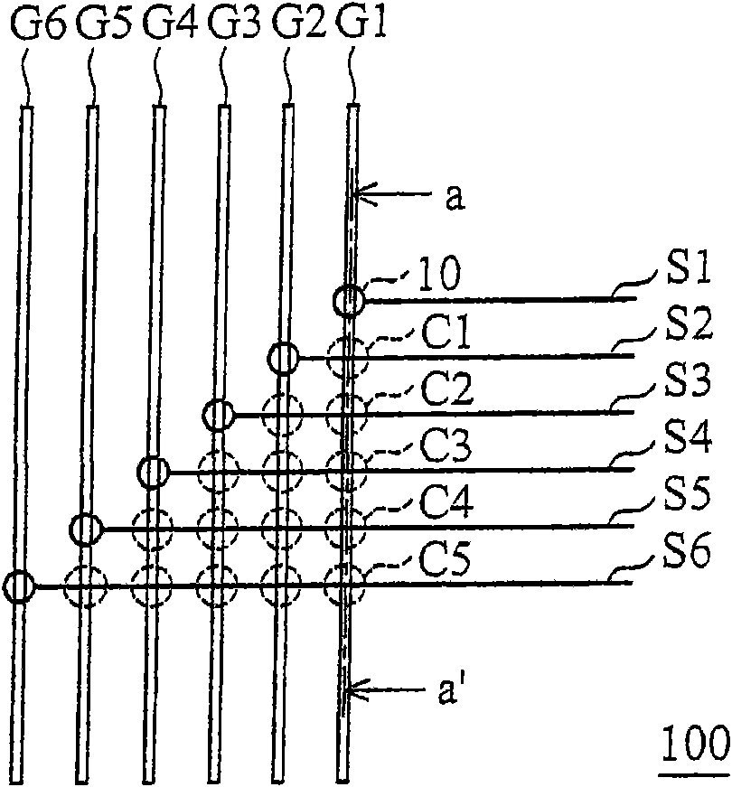
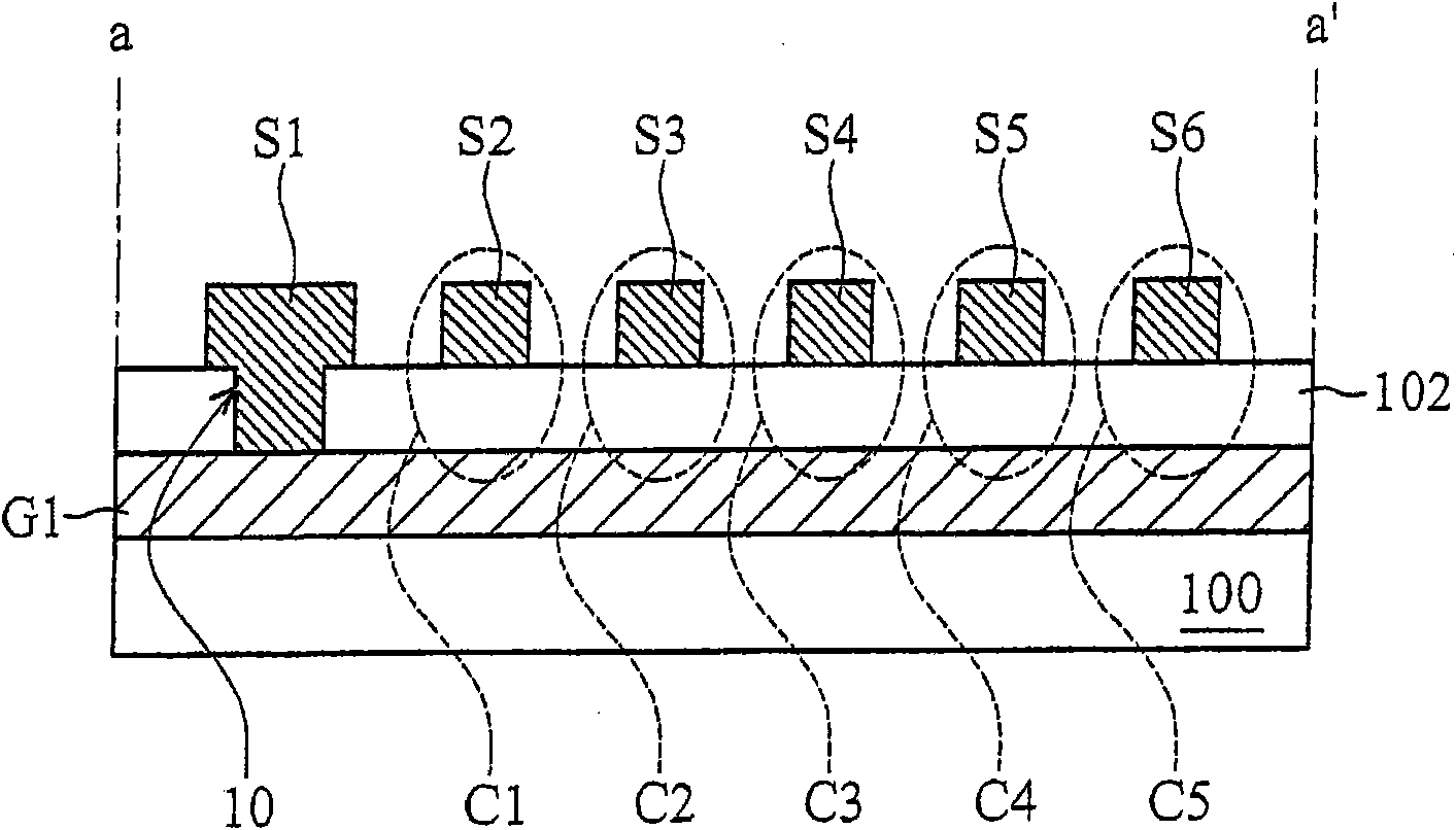
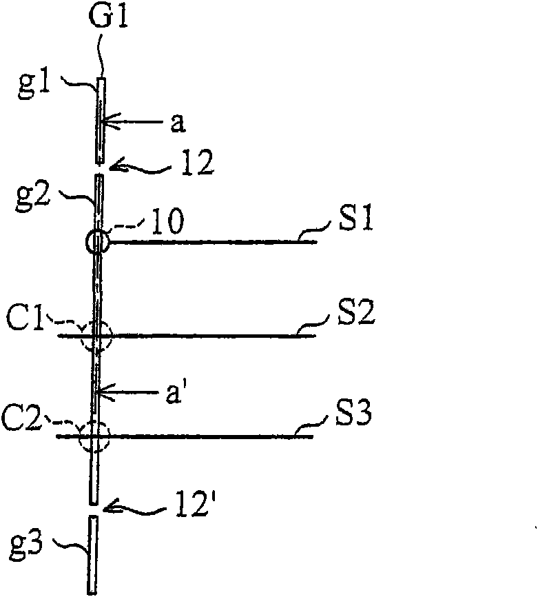
The invention provides a panel, an LCD (liquid crystal display) and a formation method of the panel, wherein the formation method of the panel comprises the steps of: providing an substrate, forming a first conductor on the substrate, forming a first insulating layer on the first conductor, forming at least one second conductor on the first insulating layer, forming a second insulating layer on the second conductor and forming a first conducting structure on the second insulating layer. The first conductor has a first part and a second part which are electrically isolated from each other; the second conductor interlaces with and is electrically isolated from the second part of the first conductor; and the first conducting structure is electrically connected with the first part and the second part. The embodiment of the invention electrically separates the part interlacing with and in cross connection with other conductors from the other part of the conductor so as to prevent the insulating layer at the cross connection position from being damaged by electro-static discharging charges, and then the embodiment forms the conductor structure so as to lead the whole conductor to be conducted. The invention can effectively avoid or reduce the damage caused by static discharge and cause each conductor to pass signals smoothly.

Description

technical field [0001] The present invention relates to a panel, a liquid crystal display and a method for forming the panel, and in particular relates to a method for forming a panel that can reduce the damage caused by electrostatic discharge. Background technique [0002] A panel (such as a display panel or a touch panel) includes many conductive lines or signal lines interlaced with each other, and these conductive lines are intersected with each other and electrically insulated by insulating layers sandwiched between each other. Taking the display panel as an example, these conductive lines are, for example, scan lines and data lines that define the pixel area or various lines in the non-pixel area, such as power lines, test lines, or drive lines. Circuits connected to integrated circuits, etc. [0003] Since many conductive lines need to be formed in the panel, in order to lay out the above-mentioned lines in a limited substrate area, some lines need to be cross-conne...

Claims


Application Information

Patent Timeline
IPC IPC(8): H01L21/768H01L23/528G02F1/133
Inventor 林威呈
Owner AU OPTRONICS CORP
Learn More