Manufacturing method of active element array substrate

A technology of an array substrate and a manufacturing method, which is applied in the field of display panels, can solve the problem of not being able to increase the storage capacitance value, etc., achieve good process yield, and avoid the effects of over-etching

Inactive Publication Date: 2009-10-21
CPT TECH GRP +1
View PDF0 Cites 8 Cited by
  • Summary
  • Abstract
  • Description
  • Claims
  • Application Information

AI Technical Summary

Problems solved by technology

[0006] The purpose of the present invention is to provide a method for manufacturing an active element array substrate, aiming to solve the problem that the prior art cannot increase the storage capacitance without affecting the aperture ratio of the pixel

Method used


Image

  • Manufacturing method of active element array substrate
  • Manufacturing method of active element array substrate
  • Manufacturing method of active element array substrate

Examples


Embodiment Construction

[0034] In order to make the object, technical solution and advantages of the present invention clearer, the present invention will be further described in detail below in conjunction with the accompanying drawings and embodiments. It should be understood that the specific embodiments described here are only used to explain the present invention, not to limit the invention.

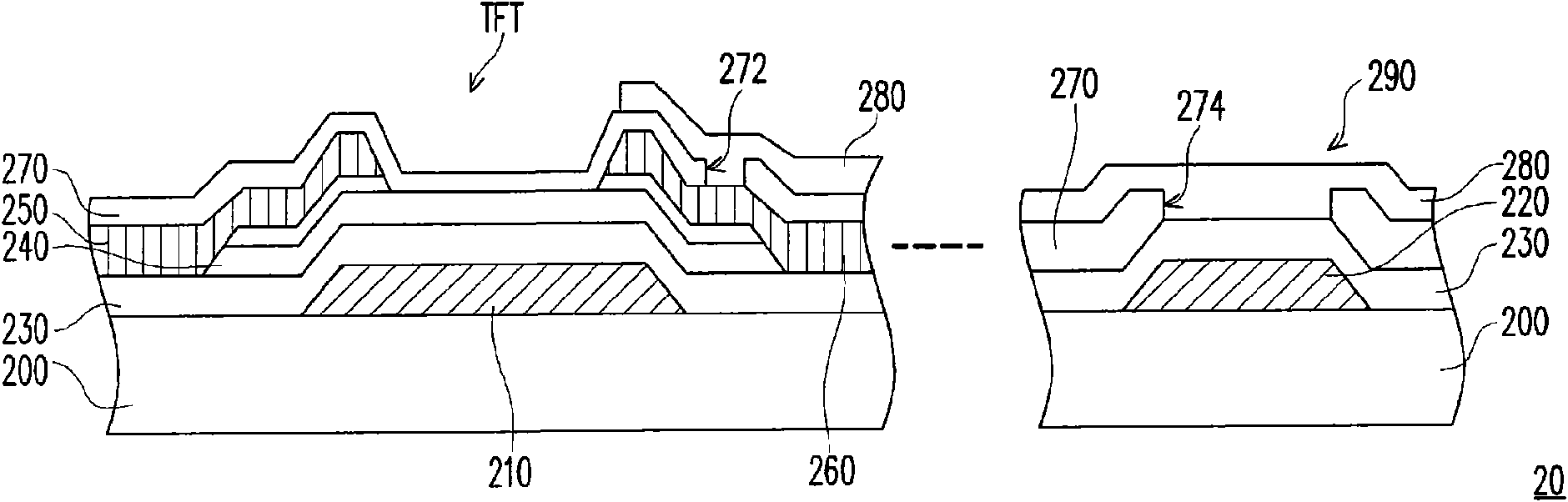
[0035] In the embodiment of the present invention, the second insulating layer above the capacitor electrode is removed at the same time when the contact window is formed. In this way, only the first insulating layer is sandwiched between the capacitor electrode and the pixel electrode to form a storage capacitor with a large capacitance value. In addition, the present invention more properly controls the process time when etching the second insulating layer to form the contact window, or uses the first / second conductive pad as the etching stop layer to well control the removal depth of the second insulati...


PUM


Abstract

The invention is applicable to the technical field of display panel, and provides a manufacturing method of an active element array substrate, comprising the following steps of: firstly, forming a gate, a capacitor electrode, a first insulating layer, a channel layer, a source electrode and a drain electrode; secondly, forming a second insulating layer on the substrate on all sides, and forming a patterning photo-resistant layer on the substrate; thirdly, removing the second insulating layer above the drain electrode and the capacitor electrode to form a contact window and an opening by taking the patterning photo-resistant layer as a mask, wherein the contact window is exposed out of the drain electrode, while the opening is exposed out of the first insulating layer positioned above the capacitor electrode; and fourthly, forming a pixel electrode on the substrate, wherein the pixel electrode passes through the contact window so as to be electrically connected with the drain electrode and filled in the opening. A storage capacitor is formed by the pixel electrode, the capacitor electrode, and the first insulating layer positioned between the pixel electrode and the capacitor electrode. In the invention, the manufacturing method of the active element array substrate has good process yield, and can avoid the occurrence of over-etching or insufficient etching.

Description

technical field [0001] The invention belongs to the technical field of display panels, and in particular relates to a manufacturing method element of an active element array substrate. Background technique [0002] The liquid crystal display panel is mainly composed of an active element array substrate, a color filter substrate and a liquid crystal layer, wherein the active element array substrate is composed of a plurality of pixel structures arranged in an array, for example. In order to control individual pixel structures, a specific pixel structure is usually selected through scan lines and data lines, and an appropriate operating voltage is provided to display display data corresponding to the pixel structure. [0003] Especially in order to maintain the operating voltage of the pixel structure and improve the display quality, usually in each pixel structure, a part of the pixel electrode covers the scanning line or the capacitor electrode to form a storage capacitor. ...

Claims


Application Information

Patent Timeline
IPC IPC(8): H01L21/82H01L21/311H01L21/02H01L21/768G02F1/1362
Inventor 黄贵伟施媚莎
Owner CPT TECH GRP
Why Eureka
Try Eureka