Semiconductor laser array device

Inactive Publication Date: 2005-12-29
MITSUBISHI ELECTRIC CORP
View PDF4 Cites 6 Cited by
  • Summary
  • Abstract
  • Description
  • Claims
  • Application Information

AI Technical Summary

Benefits of technology

[0007] An object of the present invention is to provide a semiconductor laser array device for outputting a higher power by improving efficiency of heat dissipation with a good process yield.
[0013] According to the present invention, a plurality of semiconductor laser chips are so arranged on the submount that the distance S between the centers of the chips and the thickness T of the submount satisfy the following inequality: 2×T≦S≦10×T, thereby downsizing the whole array and attaining higher efficiency of heat dissipation. Consequently, degradation of durability and characteristics can be prevented with a good process yield and a higher output power.

Problems solved by technology

Since rise in temperature of the emission region may degrade durability and characteristics, there is a certain ceiling on increasing the output power.

Method used


Image

  • Semiconductor laser array device
  • Semiconductor laser array device

Examples


embodiment 1

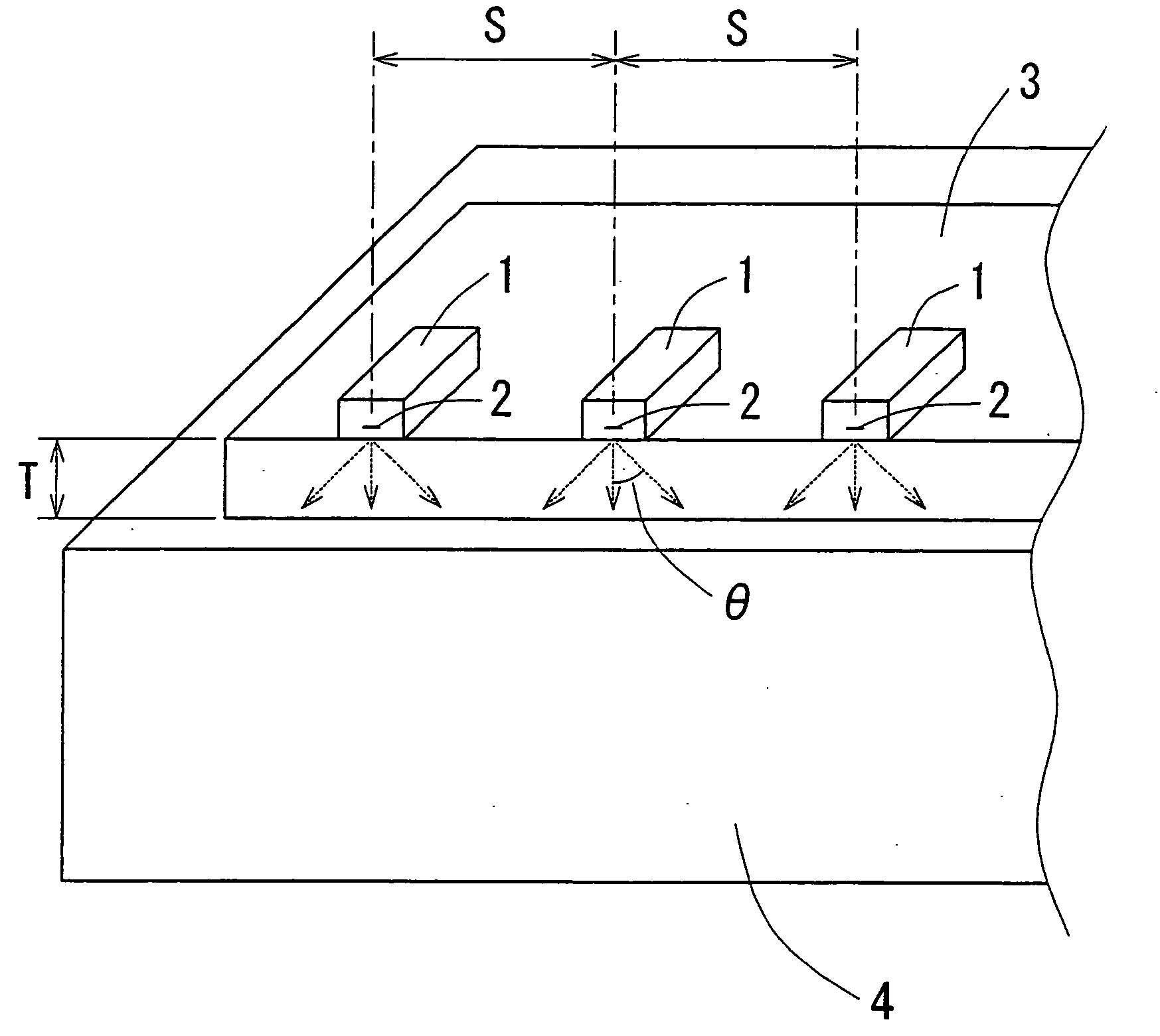
[0017]FIG. 1 is a partial perspective view showing the first embodiment according to the present invention. A semiconductor laser array device includes a plurality of semiconductor laser chips 1, a submount 3, and a heat sink 4.

[0018] The semiconductor laser chip 1 has an active layer, and a pair of cladding layers located on both sides of the active layer, in which light generated from the active layer by carrier injection passes through an emission region 2 in an end face for emitting the light exteriorly. On the upper surface of the semiconductor laser chip 1 formed is a first electrode, onto which a lead wire (not shown) is connected. On the lower surface of the semiconductor laser chip 1 formed is a second electrode, to which the submount 3 is electrically, thermally and mechanically connected by die bonding or the like.

[0019] The submount 3 is formed of an electrically and thermally conductive metal or another material having a good thermal conductivity, such as CuW (copper-...

embodiment 2

[0024] In this embodiment, the semiconductor laser chips 1 with smaller variations in oscillation wavelength are mounted in such a configuration as shown in FIG. 1.

[0025] In general, for product specifications of a semiconductor laser array device, a center wavelength λc and a full width at half maximum (FWHM) of the emission spectrum are specified. Therefore, when a plurality of semiconductor laser chips 1 are mounted, the oscillation wavelength of each chip is required to be screened.

[0026] Accordingly, it is preferable that the semiconductor laser chip 1, whose oscillation wavelength is in a range of the center wavelength λc ±4 nm, is screened to be mounted on the submount 3, thereby narrowing the emission spectrum bandwidth of the whole array and realizing a more monochromatic semiconductor laser array device.

embodiment 3

[0027] In this embodiment, the semiconductor laser chips 1 with smaller variations in oscillation threshold, external differential quantum efficiency and operating current are mounted in such a configuration as shown in FIG. 1.

[0028] In general, for product specifications of a semiconductor laser array device, a standard oscillation threshold Ith and the allowable range thereof, a standard is external differential quantum efficiency rex and the allowable range thereof, and a standard operating current Iop and the allowable range thereof, etc. are specified.

[0029] The oscillation threshold is defined as a current value at a point where a linear line during laser oscillation intersects the horizontal axis (current) in the current-optical power (I-P) characteristics of a semiconductor laser. The external differential quantum efficiency is defined as a slope ΔP / ΔI of the linear line during laser oscillation in the current-optical power characteristics. The operating current is defined...


PUM


Abstract

A semiconductor laser array device for outputting a higher power includes: a plurality of semiconductor laser chips, arranged in a predetermined pitch; a submount for mounting each semiconductor laser chip; and a heat sink for dissipating heat from the semiconductor laser chip through the submount; wherein a distance S between the centers of the chips and a thickness T of the submount satisfy the following inequality: 2×T≦S≦10×T, whereby improving efficiency of heat dissipation with a good process yield.

Description

BACKGROUND OF THE INVENTION [0001] 1. Field of the Invention [0002] The present invention relates to a semiconductor laser array device for outputting a higher power. [0003] 2. Description of the Related Art [0004] In a conventional approach using a plurality of semiconductor laser devices for outputting a higher power, a laser diode bar (LD bar) is provided with a plurality of emission regions on a single semiconductor bar, and die-bonded on a submount or a heat sink. [0005] The related prior arts are listed as follows: Japanese Patent Unexamined Publications (kokai) JP-A-2003-209313 (FIGS. 2 and 4), and JP-A-2003-158332 (FIG. 1). [0006] The LD bar has emission regions with such a small interval that heat which is generated in each emission region is transferred to the submount or the heat sink under a relatively high thermal resistance, therefore the heat hardly dissipate with high efficiency. Since rise in temperature of the emission region may degrade durability and characterist...

Claims


Application Information

Patent Timeline
IPC IPC(8): H01S3/04H01S5/00H01S5/024H01S5/40
CPCH01S5/4031H01S5/024
Inventor SHIMADA, NAOYUKISHIGIHARA, KIMIOKAWASAKI, KAZUSHIGESHIBATA, KIMITAKAYAGI, TETSUYAONO, KENICHIHANEDA, HIDEKI
Owner MITSUBISHI ELECTRIC CORP
Why Eureka
Try Eureka